In this article, we will delve into the key factors that differentiate stepper and servo motors, including their operating principles, torque characteristics, control methods, and suitability for different applications.
Technical Guides
Latest Posts

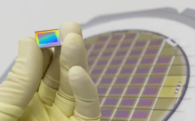
Wafer dicing separates individual integrated circuits or chips from a semiconductor wafer without damaging their delicate structures and circuits. This process is crucial for the production of electronic devices and components used in various industries, and the demand for it has increased with the development of high-performance and smaller electronic devices. Different dicing techniques, such as blade dicing, laser dicing, and plasma dicing, have been developed, and new innovations continue to emerge to address the challenges of complex semiconductor devices.
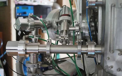
An Overview of Magnetron Sputtering and its Applications in Thin Film Growth

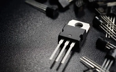
In this article, we will delve into the structure and operation of NMOS and PMOS transistors, and discuss the applications and characteristics of these essential components in electronic circuits.

In today's interconnected world, network topologies play a crucial role in determining the efficiency and reliability of communication between devices. One such network topology is the bus topology, known for its simplicity and cost-effectiveness. In this comprehensive guide, we will delve deeper into bus topology, exploring its advantages, disadvantages, applications, and the future of this network design.

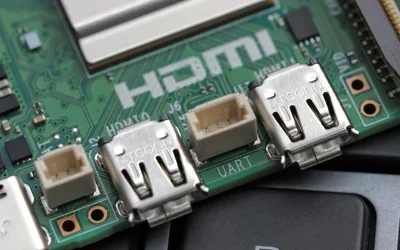
UART and SPI are key communication methods in electronics. UART is ideal for simple, long-distance connections, while SPI excels in fast data transfer. Used in GPS modules, SD cards, and microcontrollers, understanding their differences can help you choose the best for any given project.
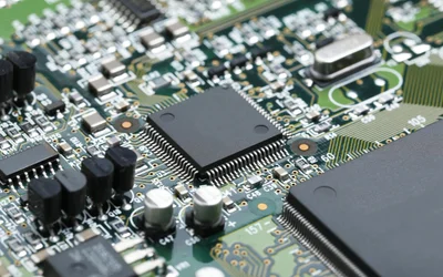
PCB mounting is critical for ensuring the lifetime and dependability of electronic products, including careful component selection and location, adherence to industry standards, and the use of high-quality materials and assembly procedures. This post will go over PCB mounting techniques, tips, and best practices and expand on crucial aspects of printed circuit board mounting.
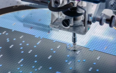
Semiconductors have become an integral part of our modern lives that relies heavily on electronics, serving as the foundation for a wide range of such devices, from smartphones and computers to medical equipment, automotive applications, and renewable energy systems.
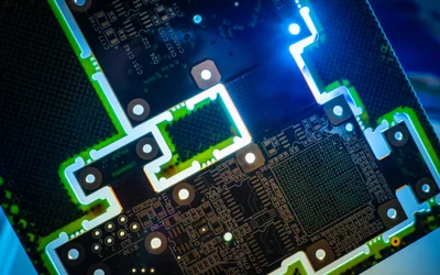
Castellated holes are extensively used in the printed circuit board (PCB) design process. This article is a detailed overview of castellated holes, covering their history, application, benefits, design attributes, challenges, and significance in modern electronic design.

SystemVerilog is the industry's leading hardware description and verification language (HDVL), offering a unified solution for digital system design and verification. This article delves into the fundamentals of SystemVerilog, highlighting its origins, key differences from Verilog, essential language elements, design constructs, and powerful verification features.

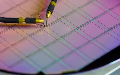
Wafer Probing is an electrical testing process conducted on semiconductor wafers after the integrated circuits are applied to the wafers. This is an essential step in the semiconductor manufacturing process that helps to determine the functionality of wafers and overall production quality. This article explores the process, importance, types, and applications of wafer probing.

Articulated robots are highly versatile and efficient robots that have the ability to mimic human arm movements for various industrial and commercial applications.

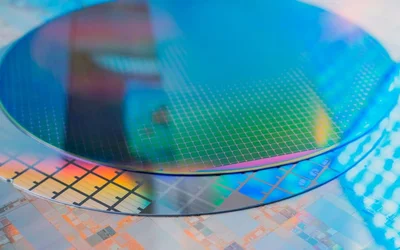
Electron beam evaporation is a physical vapor deposition process capable of applying nano-scale thin films to substrates.

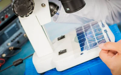
Thin film deposition is a process used to create thin film coatings on different materials. Thin films can consist of metal, semiconductors, and dielectrics, providing them with different properties. These properties translate to benefits such as electrical insulation, optical transmission, and corrosion resistance, that can be used to improve substrate performance. This article explores the processes of thin film deposition, along with its types, parameters, benefits, drawbacks, and applications.
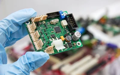
Fiducials are reference marks on a printed circuit board that achieve better assembly results.
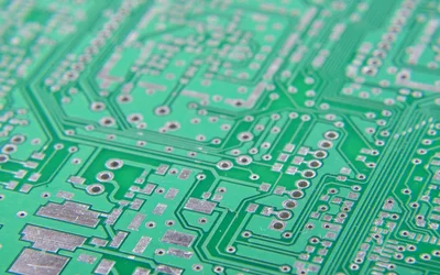
Filled vias are via holes that are completely filled and closed with conductive or non-conductive material or copper plating. The filled via is one of the many realizations of PCB via covering, specified by industry standards. This article covers the definition, benefits, processes, applications, and challenges of filled vias.
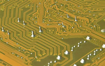
A cold solder joint is a defect caused by improper melting of solder to bond PCB electronic components. This defect can impact the functionality of a PCB assembly, and so must be carefully avoided.
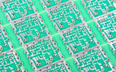
PCB Panelization is a PCB manufacturing technique. It involves the grouping of several small printed circuit boards to form a single array, which is known as a panel. Panelization is commonly employed in PCB manufacturing because it saves time and cost. This article discusses the conditions, design considerations, methods, types, and benefits of PCB panelization.

Lead-free solders offer an environment-friendly alternative to toxic lead-based solders, which were dominant in the PCB manufacturing industry till the mid-2000s.

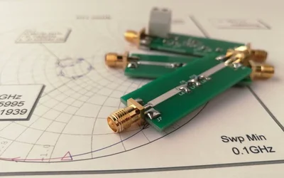
Controlled impedance in printed circuit boards involves the regulation of resistance exerted by signal traces. It is determined by characteristic factors of PCB fabrication, such as trace width and copper thickness. This article discusses controlled impedance and the essentials of its execution in PCB manufacturing.
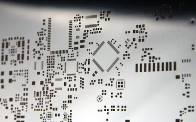
In this article, we will go over everything you need to know about PCB stencils.
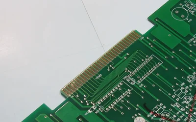
Approximately 7% of the world's gold can be found inside discarded electronic devices, in form of PCB Gold Fingers. While a tonne of Gold Ore produces just 5 grams of pure gold on average, a tonne of electronic scrap can house 300 grams of gold inside it. Here we gloss over the significance of gold fingers in the present day electronics industry and all kinds of gold fingers specifications you need to know.
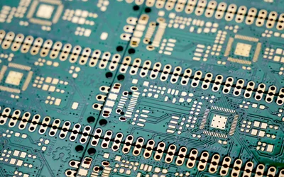
Vias go through two or more layers of PCBs to form an electrical connection. Making them right under the component’s pad saves space, reduces track inductance and simplifies design.
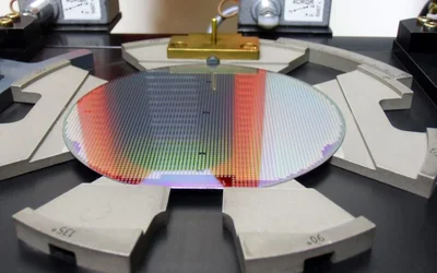
Wafer thinning is a part of the semiconductor manufacturing process. It is essentially grinding off the backside of the wafers to control their thickness and is useful for the production of ultra-thin wafers. These flattened wafers are used to effect stacked and high-density packaging in compact or microelectronic devices. This article discusses the meaning of wafer thinning, along with its various techniques and significance.
The rigid, flex and rigid-flex PCBs are all types of printed circuit boards. The rigid PCB is the traditional board and the base from which the other two variations came about, in response to industry and market needs. Flex PCBs introduced versatility to PCB fabrication and rigid-flex combines both for increased performance. Learn more about these board types, their benefits, disadvantages, and applications in this article.