What is e-beam evaporation and how does it compare to other PVD methods?
Electron beam evaporation is a physical vapor deposition process capable of applying nano-scale thin films to substrates.

27 Mar, 2023. 7 minutes read
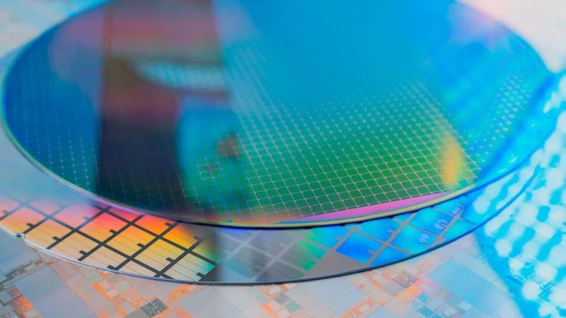
Silicone and quartz wafers can be used as substrates in e-beam evaporation
E-beam evaporation, also known as electron beam evaporation, is a physical vapor deposition (PVD) process that applies a dense, thin coating to a substrate. The process takes place under high vacuum and relies on a high-power electron beam to evaporate the coating material (the source material).
The e-beam evaporation process is used across various industries to tailor the mechanical, optical, or conductive properties of a part. In this article, we’re diving into how the e-beam evaporation process works, e-beam evaporation materials and applications, and how the technology stacks up against other thin film deposition techniques.
What is the e-beam evaporation process
In the simplest terms, the e-beam evaporation process starts by exposing a source material to an electron beam. The intense heat from the electron beam melts the source material and causes it to evaporate. The evaporated particles flow upwards in the vacuum chamber towards the substrate—which is positioned above the source material—resulting in a thin, very high-purity coating. When we say thin, we’re talking in the range of between about 5 to 250 nanometers.[1] The coating can therefore change the properties of the substrate without really influencing its dimensional accuracy.
If we look at the process in a bit more detail, e-beam evaporation is made up of a few key components:
A vacuum chamber
An electron beam source
A crucible to hold the source material
The electron beam source is a filament made from a metal like tungsten, which is heated upwards of 2,000 degrees celsius. This extreme heat causes the electrons in the tungsten filament to separate from the wire, generating kinetic energy. Magnets installed near the e-beam source generate a magnetic field, which focuses these electrons into a beam and directs it at the crucible.
The crucible can be made from metals like copper or tungsten for coating materials that require less extreme temperatures, or technical ceramics for higher temperature coating materials. We should note that while the e-beam is directed at the crucible, it only really comes into contact with the high-purity source material. The crucible is also water cooled continuously throughout the process, to prevent it from melting and mixing with the source material (which would ruin its purity).
The evaporated particles of the source material rise to the top of the vacuum chamber, where they bond with the substrate. As soon as the desired thickness has been reached—this is monitored in real time by a quartz crystal monitor—the electron beam shuts off and the system initiates a cool down and then venting sequence to relieve the vacuum pressure.
Many e-beam evaporation systems have configurations that contain multiple crucibles, which allows for substrates to be coated with different materials one after the other. The crucibles are rotated, and the e-beam evaporates the different source materials. This enables manufacturers to make multiple coating layers without having to vent the machine after each film is applied. The e-beam source power can also be controlled to accommodate different types of coating materials, each of which melts and evaporates at a different heat intensity.
Materials used in e-beam evaporation
E-beam evaporation can apply many types of material coatings onto a variety of substrates. As we saw, the process can even apply multiple different thin film materials onto a single substrate. While this isn’t an exhaustive list of e-beam evaporation materials, here are some evaporation materials and substrate materials the process can handle.
Evaporation materials
The evaporation material, also known as source material, is the raw material that is placed in the crucible and is the target of the electron beam. E-beam evaporation has the greatest material versatility when it comes to material choice for PVD processes, as it can reach higher temperatures.
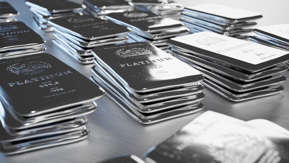
For instance, e-beam evaporation is ideal for applying coatings of metals and dielectric materials that have high melting temperatures. This includes traditional metals, such as aluminum, copper, nickel, titanium tin, and chromium; precious metals like gold, silver, and platinum; refractory metals such as tungsten and tantalum; and other materials like indium tin oxide, silicone dioxide, and more.
Substrate materials
It is possible to apply thin films to many different types of substrate. In the production of electronics, wafers made from silicon, quartz, and sapphire are common. Other possible substrates include ceramics like silicone nitride, and glass.
E-beam evaporation applications
E-beam evaporation is used in many industries, like aerospace, automotive, energy, construction, maritime, manufacturing, electronics, and consumer goods. The variety of materials compatible with e-beam evaporation makes the process incredibly versatile, enabling manufacturers to transform the properties of components and tailor them to meet certain requirements. In particular, it is used for applications that require high temperature resistance, wear and chemical resistance, or optical properties.
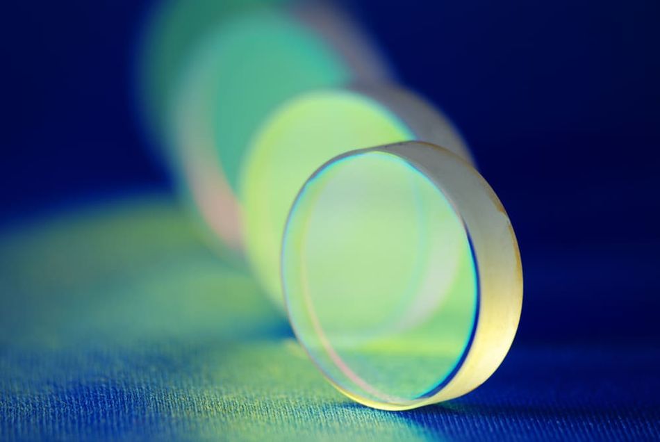
The physical vapor deposition technique can be used to different ends, using different source materials to impart different properties. For example, aerospace companies can use e-beam evaporation to add a dense, temperature-resistant coating to certain components, enhancing the original part’s ability to withstand extreme temperatures and its durability. E-beam evaporation can also be used to apply optical films for solar panels and semiconductors. In other industries, hard, corrosive-resistant coatings can be applied to protect tools and other products used in harsh environments or demanding applications.
Advantages and disadvantages of e-beam evaporation
When it comes to e-beam evaporation, there are several benefits to using the technology when thin, high-density coatings are required. Among the most notable advantages are:
E-beam evaporation has rapid vapor deposition rates of 0.1 μm/min to 100 μm/min. [2]
The process results in high-density coatings with excellent coating adhesion.
Films are very high-purity since the e-beam is concentrated solely at the source material, minimizing contamination risk from the crucible.
It offers the possibility of multi-layer deposition using various source materials, without the need for venting.
It is compatible with a wide variety of materials, including high-temp metals and metal oxides.
E-beam evaporation has a high material utilization efficiency.
There are certainly more advantages to e-beam evaporation than disadvantages, but the technology still has some limitations. For example:
E-beam evaporation is expensive: the equipment is fairly complex and the process is energy intensive.
The e-beam evaporation process is not particularly well suited to coating substrates with complex geometries: the vapor coating is best suited for line-of-sight substrates.
Comparison with other physical vapor deposition techniques
Physical vapor deposition (PVD) refers to a group of coating processes that use vacuum deposition to apply thin films onto substrates by transforming the solid coating material into a vapor (the vapor that recondenses on the substrate surface forms the coating). In addition to electron beam evaporation, there are two main PVD processes: thermal evaporation and sputtering.
Thermal evaporation vs e-beam evaporation
Thermal evaporation has much in common with e-beam evaporation, but differs in one important way. Instead of using a beam of electrons to directly heat the source material in the crucible, thermal evaporation uses an electric current to heat the crucible, which eventually melts and evaporates the source material. Thermal evaporation is well suited for metal and non-metal materials that require a lower melting temperature, while e-beam evaporation can handle higher temperature materials, such as oxides. Compared to e-beam evaporation, thermal evaporation results in less dense thin film coatings and has a greater risk of impurities, due to the crucible being heated. E-beam evaporation also has a higher deposition rate.
Sputtering vs e-beam evaporation
Sputtering, or sputter deposition, is another physical deposition process. Unlike thermal and e-beam evaporation, sputtering does not use evaporation. Instead, it uses energized plasma atoms (argon typically, because it is inert) and shoots them at a negatively charged source material. The impact of the positively energized atoms causes atoms from the negatively charged source material to break off and adhere to the substrate, resulting in a thin film. Sputtering is also performed in a vacuum.[3] Sputtering is done at a lower temperature than e-beam evaporation and has a lower deposition rate, particularly for dielectrics. That being said, sputtering provides better coating coverage for more complex substrates and is capable of high purity thin films.
Chemical vapor deposition
It’s also worth mentioning that there are also chemical vapor deposition (CVD) processes. The main difference between physical vapor deposition and chemical vapor deposition is that the former uses physical means, while the latter mixes the source material gas with a precursor substance to adhere to the substrate.[4] Despite their differences, both approaches result in the application of a very thin film layer onto a substrate.
Recommended reading: Thin Film Deposition: Everything You Need to Know
Key Takeaways
Here’s a quick overview of what we covered in this article about e-beam evaporation:
Electron beam evaporation is a type of physical vapor deposition (PVD) process that uses an electron beam to vaporize a source material and apply thin films to a substrate.
The main components of e-beam evaporation are: the electron gun; the crucible, where the source material is placed; and a vacuum chamber, which controls the pressure throughout the process.
E-beam evaporation is ideal for applying thin films of high-temperature metals and metal oxides, such as gold, chromium, platinum, and silicone dioxide.
Many e-beam systems have multiple crucibles, enabling users to apply various different coats to the substrate in a single round. This is unique amongst PVD processes.
The main benefits of e-beam evaporation are its high deposition rate, its ability to use source materials with high melting points, and its high-purity coatings.
E-beam evaporation is used in various industries to produce optical components, as well as temperature-resistant and chemically resistant parts.
References
[1] “E-Beam Evaporation.” Duke University. December 2019. [Accessed March 2023] https://www.youtube.com/watch?v=xIU1DDbDEDQ
[2] Kerdcharoen T, Wongchoosuk C. Carbon nanotube and metal oxide hybrid materials for gas sensing. InSemiconductor Gas Sensors 2013 Jan 1 (pp. 386-407). Woodhead Publishing. https://www.sciencedirect.com/science/article/pii/B9780857092366500113
[3] “Deposition”. INRF, Bion. [Accessed March 2023] https://www.inrf.uci.edu/wordpress/wp-content/uploads/day4-deposition.pdf
[4] “Explained: chemical vapor deposition.” MIT News. June 2015. [Accessed March 2023] https://news.mit.edu/2015/explained-chemical-vapor-deposition-0619