Castellated Holes: The Ultimate Guide to Their Advantages and Applications
Castellated holes are extensively used in the printed circuit board (PCB) design process. This article is a detailed overview of castellated holes, covering their history, application, benefits, design attributes, challenges, and significance in modern electronic design.

06 Apr, 2023. 6 minutes read
Introduction
Castellated holes enable reliable electric connection to another board through the edges. The half-plated semi-circular holes on the edge of a PCB are termed castellated holes. For a long time, castellated holes have been known to provide a stable electrical connection between two boards. Soon these half-plated holes simplified the process for small modules to fit on a large board. The unique manufacturing process of castellated holes has two stages where the holes are cut in half and plated with a conducting material. The top-notch features of using castellated holes in the PCB design process include robust connectivity, durability, and enhanced assembly process for complex components. The applications of castellated holes include IoT hardware, RF modules, and breakout boards.
What are Castellated Holes?
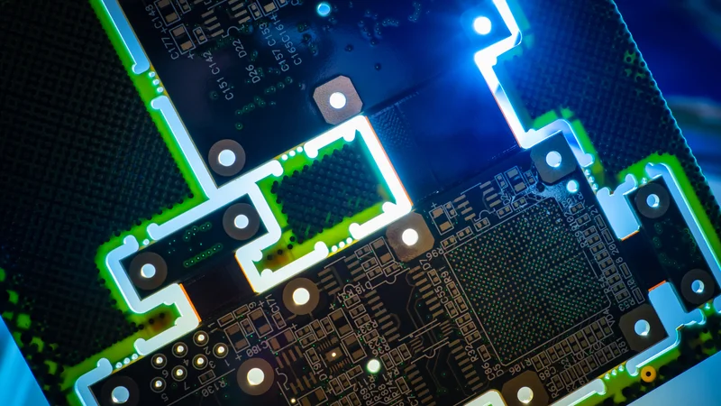
Castellated holes (plated half holes) are PCB holes cut through the edges of the board, forming a half-circular shape. These holes are then plated with a conductive material, such as gold or copper layers, to create an electrical connection between the two sides of the board. Castellated holes differ from regular vias and plated-through holes (PTH) because they are engineered to facilitate easy and reliable connections between two PCBs. Proper connection makes castellated holes suitable for modular designs and surface-mount technology (SMT) components.
History of Castellated Holes
Castellated holes date back to the early days of PCB design when engineers were experimenting with different methods of connecting circuit boards. The term "castellated" is adapted because these holes had a similar appearance to the crenellated pattern found on the top of mediaeval castle walls. Over the years, castellated holes have become more precise, reliable, and easier to work with. The process has drastically evolved with the advancements in PCB manufacturing technology. They are now a reliable alternative to a wide range of applications ranging from IoT devices to radio frequency modules and breakout boards.
Applications of Castellated holes
Castellated holes PCB are versatile enough to serve a variety of applications in telecommunications, consumer electronics, automobiles and industrial systems. Some of the most common uses for castellated holes include:
IoT Devices
The Internet of Things (IoT) is a rapidly growing industry that deploys efficient hardware to connect and communicate with each other. One of the challenges in designing IoT devices is the reliable connection of hardware to other components and systems. Castellated holes provide a stable and secure connection between PCB boards in IoT systems. IoT devices that utilize castellated PCBs include smart home systems, wearables, and sensor networks.
RF Modules
Radiofrequency (RF) PCB modules are essential components in wireless communication devices including smartphones, tablets, and laptops. Castellated holes are used in the Bluetooth and Wi-Fi modules to provide a reliable connection between the module and the main board. The unique shape and design of castellated holes ensure optimal performance for wireless communication devices. The stable connection helps to minimize signal loss and interference.
Breakout Boards
Breakout boards are small modules or PCBs designed to simplify the use of larger circuits and complex components, such as microcontrollers and sensors. These boards provide an accessible interface for connecting components to a larger system. Castellated holes are commonly used in breakout boards to provide a robust and reliable connection between the breakout board and the main PCB. The stable connection through castellated holes PCB simplifies the assembly process of complex components that may have high pin density. It is because castellated holes offer the feature of reorganisation of component pin layout to reduce the risk of damage during installation.
Benefits of Using Castellated Holes
The use of castellated holes in PCB design offers several advantages, contributing to their growing popularity among engineers and designers. These benefits include improved connectivity, enhanced durability, simplified assembly processes, and board-to-board soldering capabilities.
Castellated holes provide an excellent connection between two PCBs, ensuring minimal signal loss and optimal electrical performance. This robust connection significantly improves the overall performance and reliability of electronic devices, making them an efficient option for designers looking to maximize the efficiency and functionality of their products.
In addition to improved connectivity, castellated holes are designed to withstand the stresses of repeated connection and disconnection, making them more durable than traditional vias or plated through holes. This increased durability is particularly important in applications that require repeated hardware replacement and updating, such as IoT devices or modular electronics systems.
Lastly, castellated holes facilitate board-to-board soldering, allowing small PCB modules to act as subcircuits for larger PCBs with inverters or filters. The tight connection between the two boards ensures the quality of the solder joint and reduces the chances of dirt accumulation, making castellated holes an advantageous choice for various applications.
Design Considerations for Castellated Holes
There are several design attributes to consider during the design process for enhancing performance capabilities. Some of these factors include:
Hole Size and Spacing
Choosing the appropriate hole size and spacing is crucial for castellated hole design. The hole diameter and size should be large enough to accommodate the insertion of the component leads or pins and provide adequate clearance for soldering. If you need to reduce the required diameter on the castellated vias, ENIG surface finish is the best option. However, the surface finish largely depends upon the castellated hole application. Spacing between the number of holes should be sufficient to prevent solder bridging and ensure proper electrical isolation between connections. Designers should adhere to manufacturer guidelines and industry standards to design castellated modules. Guidelines suggest that the minimal diameter of the hole should be 0.6 mm and spacing between two castellated holes should be 0.55 mm.
Plating Thickness of plated half holes
The thickness of the plating material used in castellated holes can significantly impact their electrical performance and durability. Thicker plating materials provide a better connection but may also increase manufacturing costs and complexity. Designers should carefully consider the plating thickness requirements for their specific application. Usually, the plating thickness for holes is in the order of 20-25 microns.
Edge Clearance
Edge clearance refers to the distance between the edge of the castellated hole and the board outline. Adequate edge clearance is essential to prevent mechanical stress and potential damage to the PCB during assembly or operation. Designers should follow industry standards and adhere to manufacturer guidelines for determining the appropriate edge clearance for their specific application.
Manufacturing Challenges and Solutions
Castellated holes may have several manufacturing issues that may impact the overall quality and reliability of the final product. Some of these challenges are listed below with their possible solutions:
Alignment and Positioning
Accurate alignment and positioning of castellated holes are crucial for proper electrical connections and limiting the risk of damage during the assembly process. Design software can improve the alignment and positioning of castellated holes and check whether the tolerance levels are met.
Solder Bridging
Solder bridging is a common issue occurring in castellated hole assembly when excess solder creates unintended electrical connections between adjacent holes. To prevent solder bridging, designers should check proper hole spacing and employ solder mask designs. Furthermore, the designers must ensure that the assembly process includes appropriate soldering techniques and quality control measures.
Board Warping
When PCB is subjected to high temperatures in the manufacturing process or operation, board warping (change in PCB geometry) may occur due to the usage of castellated holes. To minimize board warping, designers should consider using materials with low coefficients of thermal expansion and implementing appropriate thermal management strategies in their designs.
Conclusion
Castellated holes are indentations in the form of semi-plated holes over the edge of a PCB board. The advantages and applications make these holes an essential tool in PCB and pad design for professionals. Besides the benefits, castellated holes require careful attention to the design considerations and have associated manufacturing challenges. Engineers and designers can incorporate castellated holes into their next electronic design project to maximize the quality of results. Castellated holes create innovative, efficient, and reliable electronic devices!
Frequently Asked Questions
To further deepen your understanding of castellated holes, here are some frequently asked questions and their answers:
What materials are used for castellated hole plating?
Castellated hole plating typically consists of copper, followed by a thin layer of nickel. The final layer may contain gold or another corrosion-resistant material. This combination provides excellent electrical conductivity, durability, and resistance to oxidation.Can castellated holes be used with flexible PCBs?
Yes, castellated holes can be used with flexible PCBs. However, special considerations should be taken into account during the design and manufacturing process to ensure proper alignment and connection between the flexible PCB and the mating board.Are there any specific design software recommendations for working with castellated holes?
Most modern PCB fabrication and design software packages like Altium Designer, OrCAD, and KiCad support castellated hole design. These software packages typically include features, tutorials, and tools specifically designed to streamline the procedures involving castellated holes.What are the cost implications of using castellated holes in PCB design?
Incorporating castellated holes into your PCB design can increase manufacturing costs due to the additional processing steps required for cutting and plating the holes. However, the benefits of improved connectivity, durability, and a simplified assembly process can often offset these additional costs, making castellated holes a cost-effective solution for many applications.How do castellated holes impact the overall size and weight of a PCB?
Castellated holes can reduce the overall size and weight of a PCB by eliminating the need for additional connectors or components to facilitate connections between boards. The assembly process simplifies to a more compact design as castellated holes contribute to smaller, lighter, and more efficient electronic devices.
References
IPC, IPC-2221B, Generic Standard on Printed Board Design, https://www.ipc.org
IPC, IPC-6012D, Qualification and Performance Specification for Rigid Printed Boards, https://www.ipc.org
in this article
1. Introduction2. What are Castellated Holes?3. History of Castellated Holes4. Applications of Castellated holes5. Benefits of Using Castellated Holes6. Design Considerations for Castellated Holes7. Manufacturing Challenges and Solutions8. Conclusion9. Frequently Asked Questions10. References