
This free-to-attend, immersive virtual event, on 22 June 2023 will cover all aspects of flexible and printed electronics, from material advancements to the development of novel deposition and manufacturing technologies.
Be the first to know.
Get our printed electronics weekly email digest.
Tagged with
Printed Electronics
ORGANIZATIONS. SHAPING THE INDUSTRY.
Latest Posts

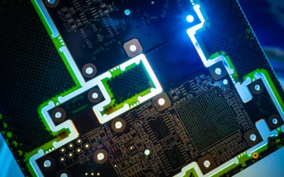
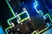
Discover what tented vias are in PCB design and how to use them effectively – covering their definition, benefits, drawbacks, and best practices from design through manufacturing!


Review of industrial applications of printed electronics - what are current successful applications?
TechBlick's presentation reviews printed electronics' industrial applications, dispelling the notion that it's solely a technology of the future. The talk showcases various commercial success stories incl. photovoltaics, displays, sensors, HMIs, 3D electronics, MLCCs, PCBs, semicon packaging, etc

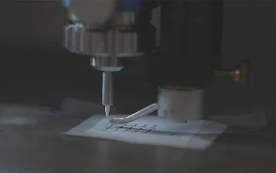
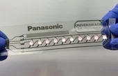
First-of-its-kind demonstration suggests a more environmentally friendly future for the electronics industry is possible
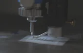
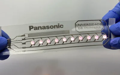
A novel stretchable film has been developed for soft & stretchable circuit / electronic solutions, outperforming existing films like TPU. Here you can learn about case studies showcasing its potential in pliable PCBs, stretchable hybrid PCBs, and truly stretchable electronics.
3 minutes read
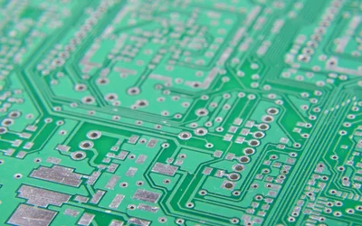
Castellated holes are extensively used in the printed circuit board (PCB) design process. This article is a detailed overview of castellated holes, covering their history, application, benefits, design attributes, challenges, and significance in modern electronic design.
In this article+talk, electrical 3D printing's technical aspects are covered, covering resin printing, circuit formation, part mounting, materials, and methods. Learn about low-temperature soldering, embedded components, and the impact on rapid prototyping and unique device manufacturing.
2 minutes read
Filled vias are via holes that are completely filled and closed with conductive or non-conductive material or copper plating. The filled via is one of the many realizations of PCB via covering, specified by industry standards. This article covers the definition, benefits, processes, applications, and challenges of filled vias.

Testing PCBs involves using various methods and tools to ensure that all the individual elements of a PCB perform optimally, making up a high-quality PCB assembly. This article delves into the methods, procedures, and requirements of PCB testing.
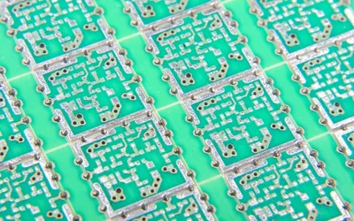
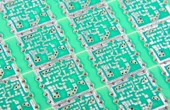
PCB Panelization is a PCB manufacturing technique. It involves the grouping of several small printed circuit boards to form a single array, which is known as a panel. Panelization is commonly employed in PCB manufacturing because it saves time and cost. This article discusses the conditions, design considerations, methods, types, and benefits of PCB panelization.
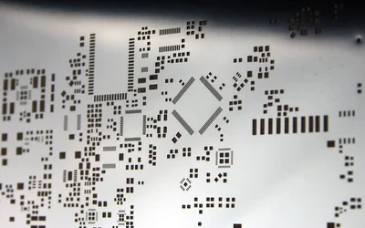
In this article, we will go over everything you need to know about PCB stencils.

This article aims to provide a comparative analysis of HASL vs ENIG, providing valuable insights to aid in making informed decisions for PCB design and manufacturing.
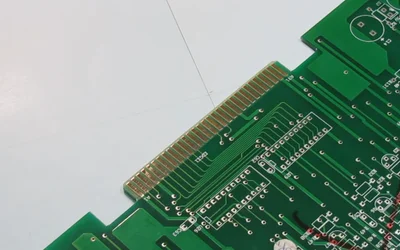
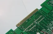
Approximately 7% of the world's gold can be found inside discarded electronic devices, in form of PCB Gold Fingers. While a tonne of Gold Ore produces just 5 grams of pure gold on average, a tonne of electronic scrap can house 300 grams of gold inside it. Here we gloss over the significance of gold fingers in the present day electronics industry and all kinds of gold fingers specifications you need to know.
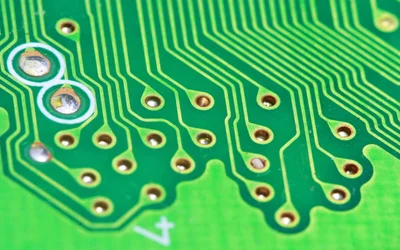
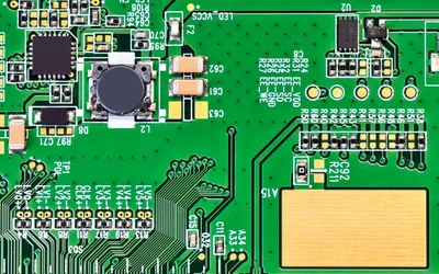
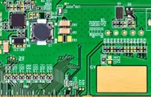
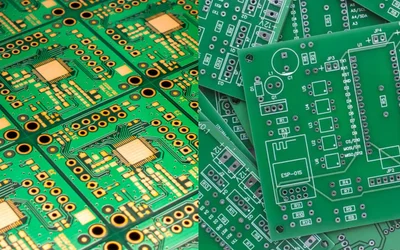
Printed Circuit Boards (PCBs) provide the foundation for the assembly of electronic components and enable the functionality of a wide range of devices. This article journeys through the requisite steps in the PCB manufacturing process, detailing the procedures involved in each.

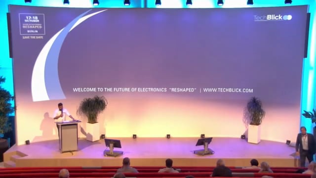
Announcing TechBlick's free-to-attend virtual conference and exhibition covering innovations in Wearable Sensors | E-Textiles | Printed Electronics & Beyond. It is a unique event with two-parallel live tracks, a live engaging exhibition floor, and 400+ attendees. See details & registration link here
2 minutes read