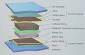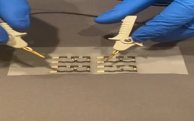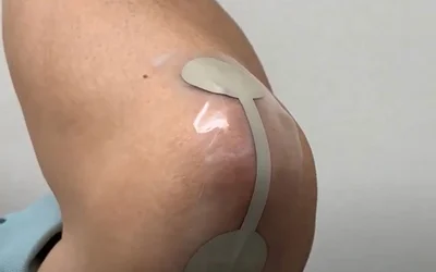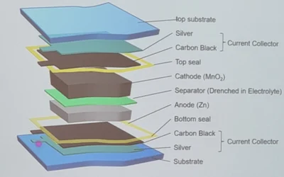
Printed batteries offer thinness and flexibility, enabling new applications, but their production is deceivingly complex. Gunter Hübner from Stuttgart Media University offered some insights at the e-Swiss conference last week.

Tagged with
Printed batteries offer thinness and flexibility, enabling new applications, but their production is deceivingly complex. Gunter Hübner from Stuttgart Media University offered some insights at the e-Swiss conference last week.
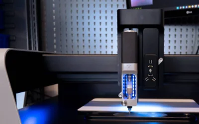
Experimenting in the world of Flexible Hybrid Electronics (FHE) comes with a variety of hurdles. Printing technologies are vastly different in terms of materials compatibility and have pros and cons that make them suitable for particular applications. Choosing materials that match the printing technology you intend to use is the most important decision you’re going to make. But what if one could print, digitally, using any paste and ink on any substrate? Read more
3 minutes read
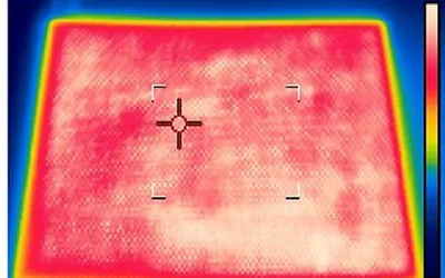
Sometimes manufacturers would like to install heating in objects that are difficult to heat. The armrest of your car. Your sporty winter coat. Bags for food delivery. Sleeping bags. etc This has been difficult to achieve until now. Read more about printed heater technology
2 minutes read
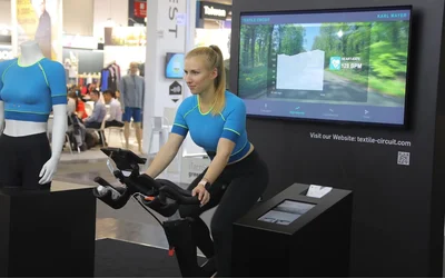
Wearable electronic textiles are a demanding environment for reliable interconnects – the ability to function with movement and survive multiple cleanings and reuse. Good adhesion is particularly challenging in these wearable and conformable electronics applications. While solders provide the most conductive electrical connection, they are rigid and require not only the addition of an underfill adhesive but usually a post bond encapsulation. This Anisotropic Conductive Epoxy, provides reliable interconnections between electronic components and circuitry on textiles with excellent structural bonding, without encapsulation, even under repeated stretching and washings. This technology has been shown as a scalable assembly process for e-Textile manufacturing in an SMT line.
5 minutes read
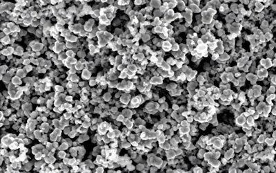
Cost of production has been a major barrier despite the fact that Cu raw material prices are far lower than Ag. This is because this large raw material cost difference does not often get translated into equally large nanoparticle dispersion or ink costs. Can this be overcome?
In general, silicone based conductive pastes are rare and the versions with AgCl fillers- needed for many medical wearable applications- are even rarer!
Warp knitting is an excellent candidate. It combines weaving and weft knitting, allowing the warp knitted fabrics to have the stability of woven fabrics and the elasticity of knitted ones.
Conformal EMI shielding is a megatrend on its way to become ubiquitous in electronics. The incumbent process is based on sputtering a tri-layer structure consisting of SUS on the EMC of the package. In these slides, you can see performance analysis and detailed cost analysis/projections.
2 minutes read
PCB layers are the copper layers within a printed circuit board, laminated between or onto layers of conductive material. These layers are stacked to enhance the functionality of electronic devices. This article explores the concept of PCB layering, the various types of layers, and their benefits.
Flexible electronics have enabled the design of sensors, actuators, microfluidics and electronics on flexible, conformal and/or stretchable sublayers for wearable, implantable or ingestible applications.
Phosphors or QDs for color conversion in LCD and microLED ? Which will win? This is an evolving technology space to watch. Here, it is shown that phosphor technology is evolving, enabling not just red but also green narrowband color conversation with small particle sizes compatible with microLEDs
2 minutes read
Molecular particle free inks can offer extreme formability and stretchability, allowing the design and production of 3D shaped and/or in-mold electronics parts with extreme curvatures and complex shapes.
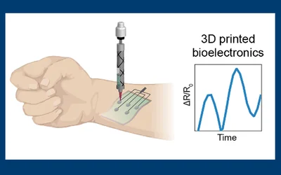
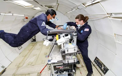
As NASA prepares to send astronauts back to the Moon to live and explore, capabilities for space-based manufacturing of sensors, circuits, and other electronics will become increasingly critical. Recent microgravity flights have helped to advance cutting-edge methods for 3D printing of electronics

4 minutes read
How to overcome the traditional limits of LDS (laser direct structuring) to metallize 2D and 3D objects made from all kinds of surfaces?
It is incredible to see the progress that organic semiconductors (OSC) have made over the past 15-20 years. Ian Jenks explains in this short 5-min presentation how they are removing the long-existing barriers to adoption of OTFT technology.