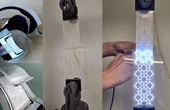
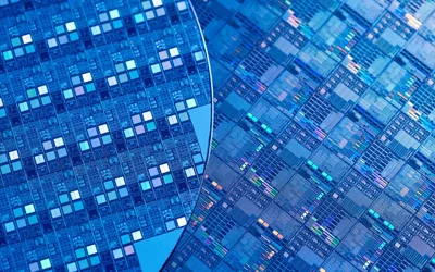
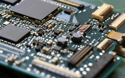
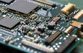
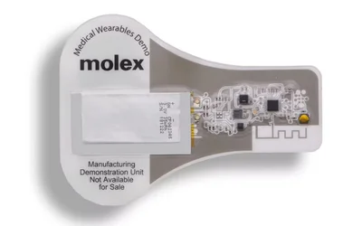
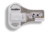
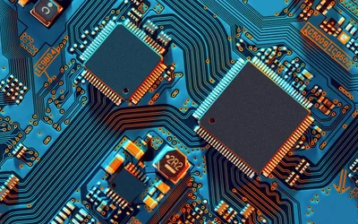
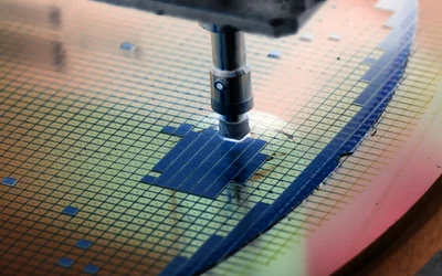
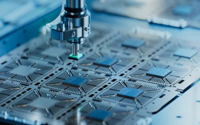
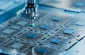
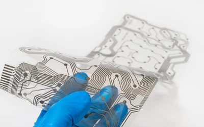
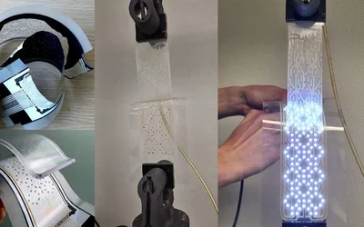
Die attach, also known as die bonding or die mount, is a process used in the semiconductor industry to attach a silicon chip to the die pad of a semiconductor package's support structure, such as a leadframe or metal can header. This article explores the fundamentals of die attach, its importance, materials, and methods used in die attach, its parameters, quality, and reliability techniques.
Tagged with
Printed Electronics
Latest Posts
Review of industrial applications of printed electronics - what are current successful applications?
TechBlick's presentation reviews printed electronics' industrial applications, dispelling the notion that it's solely a technology of the future. The talk showcases various commercial success stories incl. photovoltaics, displays, sensors, HMIs, 3D electronics, MLCCs, PCBs, semicon packaging, etc
Filled vias are via holes that are completely filled and closed with conductive or non-conductive material or copper plating. The filled via is one of the many realizations of PCB via covering, specified by industry standards. This article covers the definition, benefits, processes, applications, and challenges of filled vias.
PCB Panelization is a PCB manufacturing technique. It involves the grouping of several small printed circuit boards to form a single array, which is known as a panel. Panelization is commonly employed in PCB manufacturing because it saves time and cost. This article discusses the conditions, design considerations, methods, types, and benefits of PCB panelization.
Approximately 7% of the world's gold can be found inside discarded electronic devices, in form of PCB Gold Fingers. While a tonne of Gold Ore produces just 5 grams of pure gold on average, a tonne of electronic scrap can house 300 grams of gold inside it. Here we gloss over the significance of gold fingers in the present day electronics industry and all kinds of gold fingers specifications you need to know.