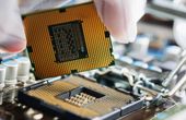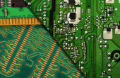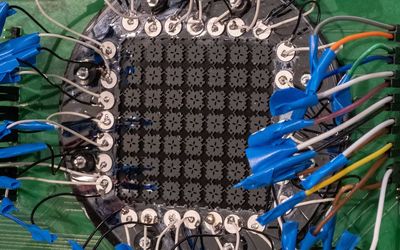


Parker and Stephen chat with James Lewis (aka the Bald Engineer) about constructing a functional computer based on the Apple II GS's Mega II chip, and also announce a contest sponsored by Mouser!

3 minutes read
Tagged with
Parker and Stephen chat with James Lewis (aka the Bald Engineer) about constructing a functional computer based on the Apple II GS's Mega II chip, and also announce a contest sponsored by Mouser!
3 minutes read
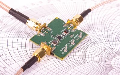
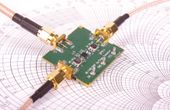
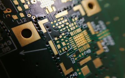
This article delves into the world of RF PCBs, exploring the design considerations that ensure signal integrity, the materials that minimize signal loss, and the intricate processes that bring these high-performance boards to life.
Understanding the need for Rigid PCB technology, capturing its manufacturing process and applications, and the innovations it has brought in modern electronics design and industrial manufacturing.
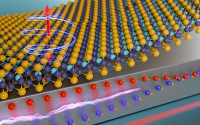
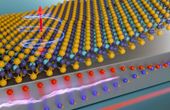
An MIT team precisely controlled an ultrathin magnet at room temperature, which could enable faster, more efficient processors and computer memories.
This article provides an in-depth exploration of the evolution, fundamental concepts, diverse types, operating principles, and practical applications of ASICs.
Startups in the hardware industry have an uphill battle to build a product that will break through in highly competitive markets. Only half survive beyond five years.
5 minutes read
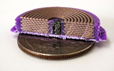
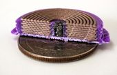
The printed solenoids could enable electronics that cost less and are easier to manufacture — on Earth or in space.
Traditional HASL uses lead, raising environmental concerns. But how does ENIG compare?
5 minutes read
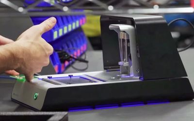
Voltera’s V-One benchtop printer is revolutionizing how electronics are developed with in-house, one-hour PCB prototyping.
In the in-depth interview, PI Vice President of Marketing Doug Bailey explains GaN technology and the new possibilities it brings to the power conversion industry.

4 minutes read
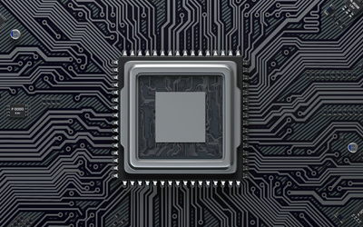
QFN packages are leadless and have short interconnects that reduce parasitic elements such as inductance and capacitance. How do they compare to other surface-mount ICs?
9 minutes read
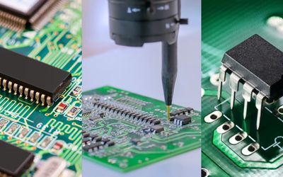
This detailed guide will cover the fundamentals of SMT vs SMD, and THT, exploring their working principle, advantages and disadvantages, comparative analysis, and choosing the right one for electronics assembly.
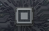
The Quad Flat No-leads (QFN) package is a type of surface-mount technology (SMT) in the electronics industry known for its compact size and high performance. This comprehensive guide explores its benefits (high performance), applications (mobile devices), and challenges (assembly, soldering).
At recent 2023 Consumer Electronics Show (CES), Sony and Honda revealed their first electric vehicle prototype, which is equipped with 45 cameras and sensors, as well as Electric Rearview Mirrors.

3 minutes read
Researchers at ETH Zurich have developed a sensor that utilises energy from sound waves to control electronic devices. This could one day save millions of batteries.

3 minutes read