Silicon Photonics: A Comprehensive Guide to the Future of Optical Communications
Exploring Silicon Photonics: Shaping the Future of Optical Communication

Last updated on 08 Dec, 2023. 11 minutes read
Introduction
Initially, integrated photonics started using materials like doped silica glass, lithium niobate, or indium phosphide as the material surface, especially for telecom and long-haul datacom applications. However, most semiconductor companies use silicon as the primary material to create integrated complementary metal-oxide-semiconductor (CMOS) circuits, achieving very high yields and low costs.
Silicon, the second most abundant element on Earth, is a cornerstone of the electronics industry due to its excellent semiconductor properties. In photonics, silicon's high refractive index contrast allows for the creation of compact photonic devices, while its transparency in the infrared region makes it suitable for optical communications.
Beyond speed and integration, silicon photonics excels in energy efficiency, a critical factor in our eco-conscious world. Silicon photonic devices consume significantly less power than their electronic counterparts, making them an environmentally friendly choice for data transmission.
Recommended Reading: Silicon Semiconductor: A Comprehensive Guide to Silicon and its Use in Semiconductor Technology.
Fundamentals of Silicon Photonics
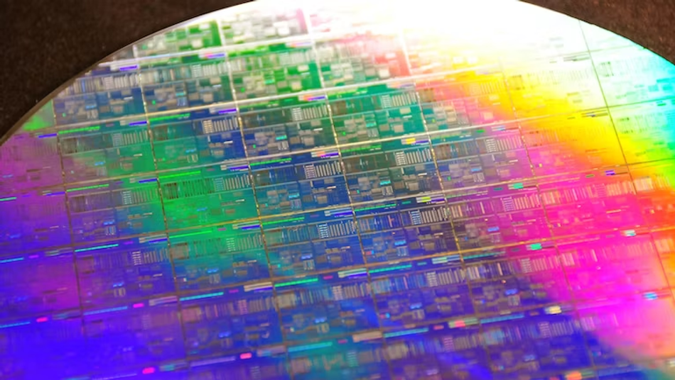
Silicon photonics (SiPh) is a material platform from which photonic integrated circuits (PICs) can be made. Silicon on insulator (SOI) wafers are used as the semiconductor substrate material, and most of the standard CMOS foundry manufacturing processes can be applied. This compatibility allows for the cost-effective mass production of silicon photonic devices, making the technology more accessible and scalable.
Optical Communications and Photonics
Photonics, the science of generating, manipulating, and detecting light, is crucial in optical communications. Even though it has evolved significantly with advancements in materials and devices, the emergence of silicon photonics has pushed this progress further by offering a new level of integration, performance, and scalability in optical communication systems.
Silicon photonics can deliver high-speed, energy-efficient, and integrated solutions by exploiting silicon's unique properties and photonics principles. This technology is already revolutionizing communications including data center interconnects, artificial intelligence, long-haul telecommunications, and high-performance computing.
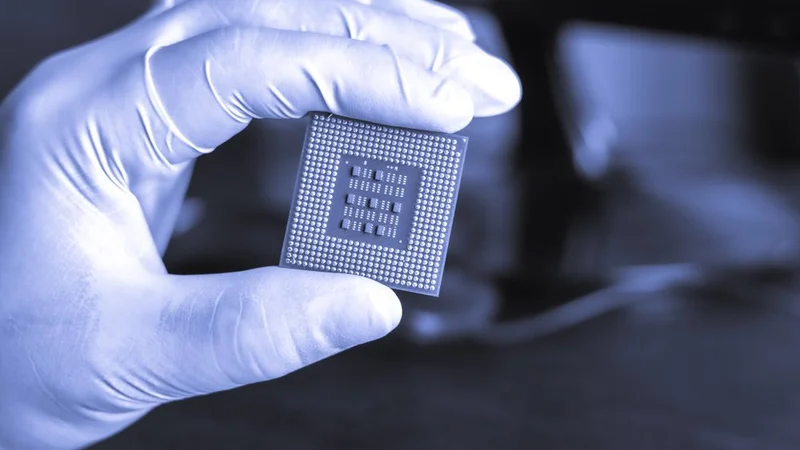
Silicon as a Material for Photonics
Silicon is a cornerstone of the electronics industry due to its excellent semiconductor properties. Its atomic structure, which comprises four valence electrons, allows it to form covalent bonds with other silicon atoms, creating a stable and robust crystal lattice.
In the field of photonics, silicon's properties offer several advantages. Notably, it has a high refractive index contrast, about 3.5 at infrared wavelengths, meaning it can bend or slow down light more effectively than many other materials used in photonics. This high refractive index contrast allows for the creation of compact photonic devices with tight light confinement, leading to smaller device footprints and higher integration densities.
Moreover, silicon's transparency in the infrared spectrum, specifically at wavelengths around 1.3 and 1.55 micrometers, aligns well with the wavelengths commonly used in optical communications. This compatibility enables silicon-based devices to transmit high volumes of data over long distances without losing the signal significantly.
Silicon's compatibility with existing CMOS fabrication processes is another significant advantage. CMOS technology is the backbone of the semiconductor industry, and its well-established fabrication processes can be leveraged to produce silicon photonic devices at scale, reducing costs and accelerating the adoption of the technology.
However, silicon faces challenges in photonics due to its indirect bandgap, leading to inefficiencies in emitting light, a critical function in photonic devices. Overcoming this limitation has been a significant focus of research in the field, including companies such as IBM and Intel, with approaches such as silicon alloys and hybrid integration techniques showing promise.
Despite these challenges, the advantages of silicon in photonics far outweigh its limitations. Its unique properties, combined with its compatibility with CMOS fabrication processes, position silicon as a leading material for the future of photonics.
Image credit: Cardiff University.
Recommended Reading: An introduction to Integrated Photonics.
Key Components of Silicon Photonic Devices
Silicon photonic devices are designed and optimized to manipulate light in various ways, enabling the device to perform multiple functions, from guiding and modulating light to detecting and converting it into electrical signals. One of the primary optical components of a silicon photonic device is the waveguide. Waveguides are structures, typically made of silicon, that guide light from one point to another, analogs to wires that conduct electrical signals in electronic devices.
Another critical component is the modulator. Modulators are devices that control the properties of light, such as its amplitude, phase, or frequency, to encode information. Completing this set of components are the photodetectors, pivotal in converting light into electrical signals, enabling interaction with electronic systems. These photodetectors utilize the photoelectric effect in silicon to generate electron-hole pairs, eventually collected as electrical current.
Waveguides
Waveguides, the interconnects between photonic devices in the circuit, are made from a silicon core and come in different styles, like a rib or strip, and have the oxide from the SOI substrate as bottom cladding and air or another layer of silicon oxide as top cladding. There are several types of waveguides used in silicon photonics. For instance, strip waveguides offer tight light confinement and low propagation loss, making them suitable for high-density integration. On the other hand, slot waveguides can enhance light-matter interaction, making them ideal for applications such as sensing and modulation.
Its performance is influenced by several factors, including the waveguide geometry, material composition, and fabrication process. These factors can affect the waveguide's propagation loss, mode confinement, and dispersion characteristics, requiring careful design and optimization.
Modulators
Modulators work by altering one or more characteristics of a light wave, such as its amplitude, phase, or frequency, in response to an external signal. The modulation of light is possible due to the electro-optic effect, where the refractive index of a material changes in response to an applied electric field. By applying a voltage across the modulator, the refractive index of the silicon can be altered, causing a corresponding change in the phase or amplitude of the light passing through it.
Multiple types of electro-optic modulators are used in silicon photonics, including Mach-Zehnder interferometers and ring resonators. Mach-Zehnder interferometers split light into two paths, adjust the phase in one path, and then merge them to control how light combines. On the other hand, ring resonators work by trapping light in a circular waveguide and modulating its resonance condition to control light transmission.
The performance of a modulator depends primarily on the modulation speed, extinction ratio, and power consumption. Modulation speed refers to how quickly the modulator can switch between different states, with faster speeds enabling higher data rates. The extinction ratio, the power ratio in the 'on' state to the 'off' state, determines the modulator's ability to distinguish between different data levels. Power consumption, however, is particularly crucial in tightly packed systems where managing heat is a meaningful roadblock.
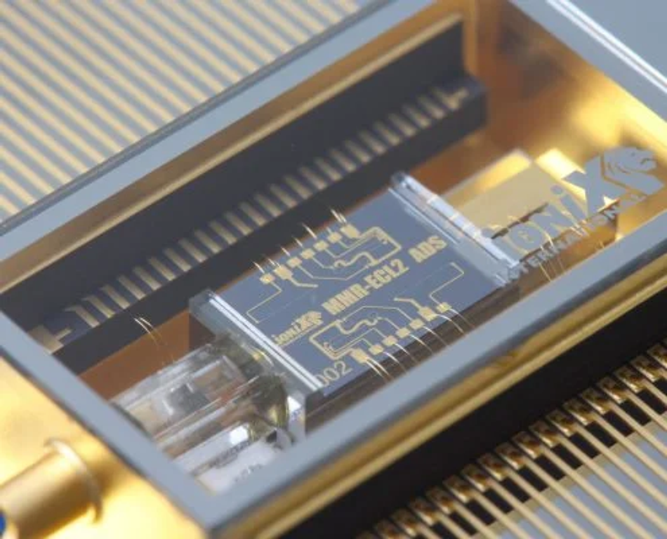
Photodetectors
Photodetectors are the interface between the optical and electronic domains. They convert incoming light into electrical signals, enabling the device to process and interpret the transmitted data. Due to the principle of the photoelectric effect, photodetectors absorb light within a material, generating electron-hole pairs that form the basis for electrical current collection.
This component is typically made of silicon and operates in the infrared region, specifically at wavelengths around 1.3 and 1.55 micrometers. It coincides with the minimum loss window of silica-based optical fibers and allows the photodetectors to convert incoming light into electrical signals with minimal loss efficiently.
Several types of photodetectors can be used in silicon photonics, such as p-i-n photodiodes and avalanche photodiodes. P-i-n photodiodes create a depletion region between a p-type and an n-type semiconductor, where light absorption generates electron-hole pairs that are separated by the electric field, creating a photocurrent. In contrast, avalanche photodiodes leverage the multiplication effect, where light absorption triggers a chain reaction of electron-hole pair generation, leading to a significant increase in the photocurrent.
Its performance is based mainly on responsivity, bandwidth, and noise characteristics. Responsivity refers to the photodetector's ability to convert incoming light into electrical current, with higher responsivity leading to stronger electrical signals. Bandwidth determines the range of frequencies the photodetector can operate at, with high bandwidths enabling higher data rates. Noise characteristics, such as dark current and shot noise, can affect the photodetector's signal-to-noise ratio and, ultimately, its sensitivity and data integrity.
Image credit: PhotonDelta.
Recommended Reading: Boosting light power revolutionizes communications and autopilot.
Silicon Photonic Integration
Silicon photonic integration combines multiple photonic components, such as waveguides, modulators, and photodetectors, onto a single silicon chip. This integration is similar to electronic components in an integrated circuit (IC) but with light as the information carrier instead of electrical current. Photonic integrated circuits aim to create compact, high-performance, and cost-effective photonic devices that can be produced at scale.
An advantage of silicon photonic integration is its potential to pack many components tightly. Due to silicon's high refractive index, photonic components can be made very small, allowing many components to be integrated onto a single chip. This high-density on-chip integration can lead to devices with high functionality and performance.
However, silicon photonic integration also presents several challenges. These include the need for precise alignment of components, the management of thermal effects due to high-density integration, and the handling of light sources, given silicon's inefficiency at emitting light.
Monolithic Integration
Monolithic integration is a type of silicon photonic integration where all the photonic components are fabricated on a single silicon chip in a single process flow. This approach ensures high compatibility and alignment between the components, leading to high device performance and reliability.
A significant advantage of monolithic integration is the potential for high yield and scalability. By fabricating all components together, the process becomes more efficient and scalable, vital in commercial applications where cost-effectiveness and large-scale production matter. Another benefit is the potential for high device performance. Since all the components are fabricated on the same chip, they can be closely matched and aligned, reducing signal loss and improving device performance.
However, monolithic integration also presents several challenges. These include the need for complex fabrication processes, the management of thermal effects due to the proximity of components, and the handling of different material properties and requirements for other components.
Hybrid Integration
Hybrid integration integrates components from different materials, each optimized for specific functions, such as light emission, modulation, or detection. By combining the best of different materials and technologies, hybrid integration can enable new functionalities and performance characteristics that are not possible with monolithic integration alone.
This device design flexibility allows designers to choose the best materials and processes for each component, potentially leading to higher overall device performance. For example, hybrid integration enables the incorporation of efficient light-emitting materials, such as indium phosphide, into silicon photonic devices, overcoming the limitations of silicon's indirect bandgap.
Additionally, hybrid integration has the potential for improved thermal management. Since components are fabricated separately, they can be spaced apart on the chip or substrate, reducing the risk of thermal crosstalk and allowing for more effective heat dissipation. This can be particularly important in high-density integration scenarios, where thermal management is a critical challenge.
The main challenge is the need for precise alignment and bonding of the different components. This process can be complex and time-consuming, potentially impacting yield and scalability. Additionally, using multiple materials and fabrication processes can introduce compatibility issues and increase the complexity of the overall device design.
Recommended Reading: Integrated Photonics: Comprehensive Guide to Optical Communication.
Applications of Silicon Photonics
Silicon photonics technology has various applications across different industries thanks to its ability to deliver high-speed, energy-efficient, and integrated solutions. By taking advantage of the unique properties of silicon and the principles of photonics, silicon photonic devices can address the growing demand for high-speed data transmission and enable new functionalities.
Data Centers and High-Speed Communications
One of the primary applications of silicon photonics is in data centers and high-speed communications. The rapid growth of data traffic, driven by the increasing use of cloud services, streaming media, and the Internet of Things (IoT), has created a need for faster and more efficient data transmission solutions.
Silicon photonic devices, such as transceivers and optical switches, can significantly improve the performance of data center interconnects by enabling higher data rates, lower latency, and reduced power consumption compared to traditional electronic devices. For example, silicon photonic transceivers can support data rates of up to 400 gigabits per second (Gbps) and beyond while consuming less power than their electronic counterparts.
In high-speed communications, silicon photonics can also be crucial in long-haul telecommunications and high-performance computing. Its ability to transmit data at high speeds over long distances with minimal signal loss makes it an attractive option for upgrading existing optical networks and enabling next-generation communication systems.
Sensing and Imaging
The technology's ability to manipulate light at the nanoscale opens up new possibilities for creating highly sensitive and compact sensors for various applications, including environmental monitoring, industrial process control, and biomedical diagnostics.
In environmental monitoring, these sensors can detect and measure various ecological parameters, such as temperature, humidity, and gas concentrations. These sensors operate by detecting alterations in these factors through light interactions. For instance, lidar, which stands for light detection and ranging, is a remote sensing method that uses light as a pulsed laser to measure variable distances to the Earth. These light pulses, combined with other data recorded by the airborne system, generate precise, three-dimensional information about the shape of the Earth and its surface characteristics.
Image credit: National Oceanic and Atmospheric Administration (NOAA).

Photonics sensors can monitor industrial process parameters in real-time, such as pressure, flow rate, and chemical composition. These sensors can offer high sensitivity, fast response times, and resistance to harsh industrial environments, making them ideal for ensuring process efficiency and safety.
Regarding biomedical diagnostics, silicon photonics can enable the development of lab-on-a-chip devices that can perform complex biochemical analyses on a single chip. These devices use light interactions with biological samples to detect and measure various biomarkers, such as proteins, DNA, and cells. For example, a biosensor might use the change in refractive index caused by the binding of a target biomolecule to a sensor surface to detect the presence of that biomolecule.
This technology can enable the development of high-resolution, compact, and cost-effective imaging systems. These systems can leverage these devices' waveguiding and interference properties to manipulate light in ways that enhance imaging capabilities. For instance, an imaging system might use an array of optical waveguides to focus light onto a sample, enabling high-resolution imaging.
Biomedical Applications
Biomedical studies, in general, can get valuable insights by analyzing nanoscale interactions with silicon photonics. Silicon photonics can be used to develop lab-on-a-chip systems, allowing complex biochemical analyses on a single chip.
These systems can detect and measure various biomarkers, such as proteins, DNA, and cells, enabling the rapid and accurate diagnosis of diseases. For instance, a biosensor might use the change in refractive index caused by the binding of a target biomolecule to a sensor surface to detect the presence of that biomolecule. This could enable the early detection of diseases such as cancer, improving patient outcomes.
In therapeutics, such devices can be used to develop targeted drug delivery systems and photothermal therapies. For example, nanoparticles can be designed to absorb light at specific wavelengths, generating heat that can kill cancer cells or trigger the release of drugs. This could enable more effective and less invasive treatments for cancer-related diseases.
Recommended Reading: Key Application Areas for Integrated Photonics.
Conclusion
Silicon photonics is a transformative technology with great promise for the future of optical communications and various other applications. By leveraging silicon's unique properties and photonics principles, this technology can deliver high-speed, energy-efficient, and integrated solutions that can revolutionize industries such as data centers, artificial intelligence, telecommunications, sensing and imaging, and biomedical applications. Despite the challenges associated with integration and device fabrication, ongoing research and development efforts push the boundaries of what is possible, paving the way for a more connected and data-driven future.
Frequently Asked Questions (FAQs)
1. What is silicon photonics?
Silicon photonics is a technology that combines the properties of silicon with the principles of photonics to create highly efficient, compact, and high-speed photonic devices for optical communications and other applications.
2. Why is silicon used in photonics?
Silicon is used in photonics due to its high refractive index, transparency in the infrared region, and compatibility with existing complementary metal-oxide-semiconductor (CMOS) fabrication processes.
3. What are the main components of silicon photonic devices?
The main components of silicon photonic devices include waveguides, modulators, and photodetectors.
4. What are the advantages of silicon photonic integration?
Silicon photonic integration offers several advantages, including high-density integration, compatibility with CMOS fabrication processes, and the potential for high-performance, cost-effective photonic devices.
5. What are some applications of silicon photonics?
Silicon photonics has various applications across various industries, including data centers and high-speed communications, sensing and imaging, and biomedical applications.
6. What is Co-Packaged Optics?
Co-Packaged Optics (CPO) is an advanced integration of optics and silicon on a single packaged substrate to address next-generation bandwidth and power challenges. CPO brings together a wide range of expertise in fiber optics, digital signal processing (DSP), switch application-specific integrated circuits (ASICs), and state-of-the-art packaging and testing to provide disruptive system value for the data center and cloud infrastructure.
References
National Oceanic and Atmospheric Administration, 2023. “What is lidar?”
SLT, 2023. “Optical Interconnect Vs. Electrical Interconnect: All You Need to Know”
Synopsys, 2021. “What is Silicon Photonics?”
Jessica Miley, 2020. “An introduction to Integrated Photonics”
Saliha Malik, 2023. “Integrated Photonics: Comprehensive Guide to Optical Communication”
Cardiff University, 2023. “Newport Wafer Fab Ltd”
PhotonDelta, 2022. “What is a Photonic Integrated Circuit?”