PVD Coating in Semiconductors: A Comprehensive Guide
This article offers an in-depth view of PVD coating in semiconductors, their underlying technology, materials, and applications crucial in today's rapidly evolving technological landscape.

13 Dec, 2023. 16 minutes read
PVD Coating in Semiconductors
Introduction
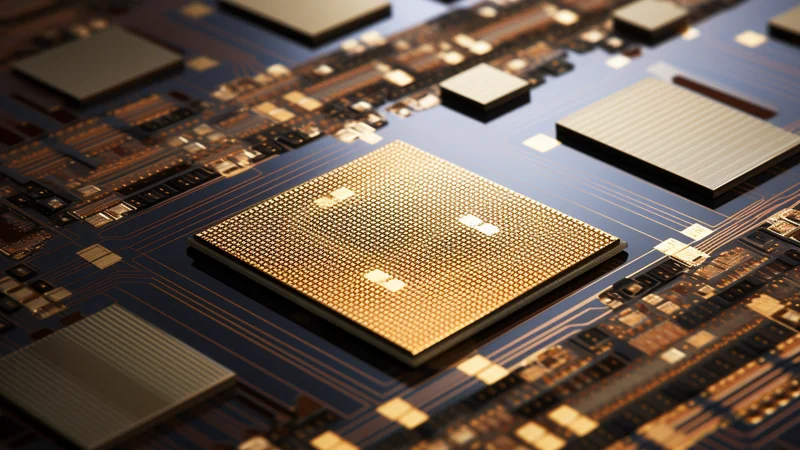
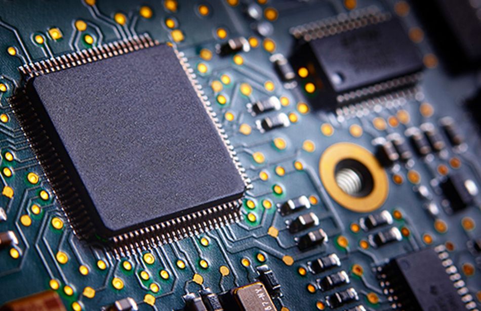
In the ever-evolving landscape of semiconductor technology, Physical Vapor Deposition (PVD) coating stands as a cornerstone technique, pivotal in the fabrication of electronic devices. The process involves the transfer of material from a solid or liquid source to a substrate surface. The material is vaporized in a vacuum chamber and then condensed onto the substrate.
PVD coating is used to deposit metals, such as aluminum or copper, and insulators, such as silicon dioxide or nitride. The deposited films play crucial roles in the fabrication of semiconductor devices, serving as conductive pathways, barriers, or insulators. This versatile technique employs physical processes such as sputtering or evaporation to deposit materials at an atomic or molecular level.
PVD coating stands out for its high purity and uniformity. These qualities are vital for reliable semiconductor performance. However, it requires complex, costly high vacuum conditions and precise control. Its scalability is a major advantage for mass production. With an increasing demand for smaller, faster, and more energy-efficient semiconductor devices, PVD coating is becoming inevitable.
The Science Behind PVD Coating
Physical Vapor Deposition (PVD) is a process where materials are transferred at an atomic level, based on thermodynamics and kinetics. Carried out in a high vacuum chamber with a pressure approximating outer space at 10-2 to 10-6 Torr (102 to 104 millibar), the process usually takes place between 50 and 500 Degrees C. [1] The source material is vaporized, often by heating, changing it from solid or liquid to gas. These vaporized atoms or molecules then travel across a vacuum chamber to the substrate, forming a thin film.
The film's thickness is influenced by the source material's vapor pressure and the substrate's temperature. Factors like the source material type, temperature, and pressure, along with substrate characteristics, affect the film's composition, structure, and morphology. By controlling these factors, it is possible to tailor the properties of the film to meet specific requirements.
The Role of Vacuum in PVD Coating
A vacuum environment plays a crucial role in the PVD coating process. First, it removes air and other gases from the chamber, preventing unwanted reactions between these gases and the source material or the substrate. This is particularly important for the deposition of reactive materials, such as metals, that can oxidize in the presence of oxygen.
Second, a vacuum environment facilitates the vaporization of the source material and the migration of the vaporized atoms or molecules toward the substrate. In a vacuum, the mean free path of the atoms or molecules (the average distance they can travel without colliding with other particles) is significantly increased. This allows the atoms or molecules to travel directly from the source to the substrate, resulting in a uniform and high-quality film. [2]
Third, a vacuum environment allows for precise control over the process parameters. By adjusting the vacuum level, it is possible to control the rate of deposition and the properties of the film. For instance, a higher vacuum level can lead to a higher deposition rate and a denser film, while a lower vacuum level can result in a slower deposition rate and a more porous film.
Vacuum technology is a critical aspect of PVD coating, requiring a deep understanding of its principles and practical considerations. Maintaining a vacuum environment can be challenging, requiring specialized equipment, such as vacuum ovens, pumps, and vacuum gauges, and careful monitoring of the process parameters. Any leaks in the chamber or fluctuations in the vacuum level can adversely affect the quality of the film.
The Role of Vapor in PVD Coating
Vapor plays a pivotal role in the Physical Vapor Deposition (PVD) process. The source material, whether it's a metal or a compound, is transformed into a vapor phase. This transformation is typically achieved through the application of heat or by bombardment with ions (sputtering). The vaporization process is a critical step in PVD coating, as it allows the source material to be transported to the substrate.
The vaporized atoms or molecules then traverse the vacuum chamber and reach the substrate. [3] The movement of these particles is driven by the pressure differential between the source and the substrate. As these particles reach the substrate, they lose their energy and condense, forming thin-film coatings on the substrate surface.
The characteristics of the vapor, such as its composition and energy, significantly influence the properties of the deposited film. For instance, the energy of the vaporized particles affects the adhesion and density of the film. High-energy particles can create a film with strong adhesion and high density, which are desirable properties for many applications in the semiconductor industry.
The composition of the vapor is crucial for achieving the desired composition of the deposited film. Careful control over the vaporization process is required, which can be challenging for some materials due to issues such as differential vapor pressures or reactivity. Understanding the role of vapor in PVD coating and how to control its properties is essential for achieving high-quality films with the desired characteristics.
Recommended Reading: Thin Film Deposition: Everything You Need to Know
Types of PVD Coating Processes Used in Semiconductors
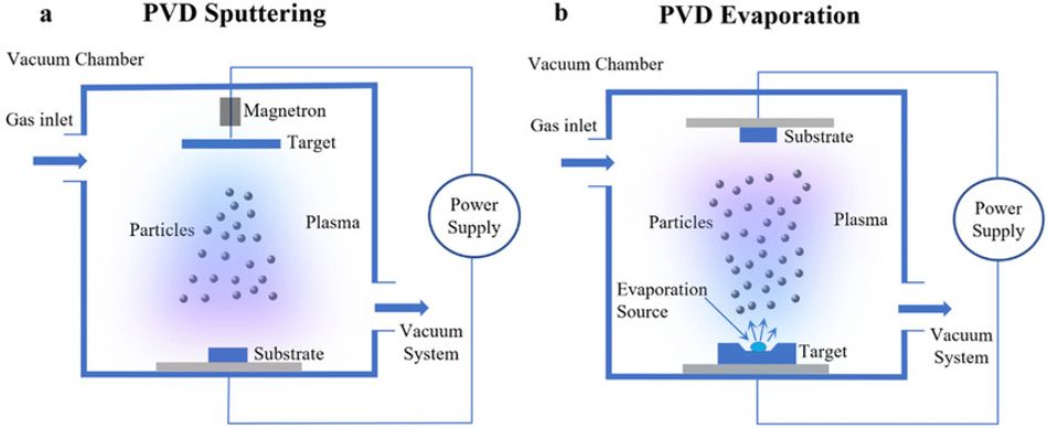
In the semiconductor industry, there are two primary types of Physical Vapour Deposition (PVD) processes: sputtering and evaporation. Both processes involve the transformation of the source material into a vapor state, which is then transported across a vacuum chamber to the substrate. [4] However, they differ in the method used to vaporize the source material and in the characteristics of the resulting film.
Both sputtering and evaporation have their advantages and disadvantages. Sputtering can deposit a wider range of materials and achieve better film uniformity, but it requires more complex equipment and higher process control. Evaporation is simpler and more cost-effective, but it may be limited in its ability to deposit certain materials or to achieve certain film properties.
Cathodic arc PVD is also a specific type of PVD process that utilizes a high-current electrical arc to vaporize a source material. This technique offers distinct advantages for semiconductor applications, particularly in terms of corrosion protection.
Sputtering
Sputtering is a PVD process that involves the bombardment of the source material with high-energy ions. These ions are typically generated by a plasma, which is created by applying a high voltage between the source material (also known as the target) and the substrate.
When the ions strike the target, they dislodge atoms from its surface. These atoms then travel across the vacuum chamber and condense on the substrate, forming a thin film. The energy of the ions, the pressure of the plasma, and the distance between the target and the substrate are among the factors that influence the rate of sputtering and the properties of the film. [5]

Sputtering is widely used in the semiconductor industry due to its versatility and precision. It can deposit a wide range of materials, including metals, alloys, and compounds, onto various types of substrates. It also allows for precise control over the composition and coating thickness of the film, which is critical for the fabrication of semiconductor devices.
However, sputtering also presents certain challenges. It requires high vacuum conditions and a stable plasma, which can be complex and costly to maintain. It also requires a high-quality target, as any impurities in the target can be incorporated into the film. Despite these challenges, sputtering remains a key process in semiconductor manufacturing, with ongoing research and development aimed at improving its capabilities and efficiency.
Recommended Reading: Magnetron Sputtering: A Versatile Thin Flim Deposition Technique
Evaporation
Evaporation is another PVD process used in the semiconductor industry. It involves heating the source material to high temperatures, causing it to vaporize. The vaporized atoms or molecules then travel across the vacuum chamber and condense on the substrate, forming a thin film. Evaporation is typically used for the deposition of pure metals, as it can achieve high deposition rates and high-purity films.
The evaporation process can be carried out using various methods, such as resistive heating, electron beam heating, or induction heating. In resistive heating, an electric current is passed through the source material, generating heat due to the material's resistance. Electron beam heating involves bombarding the source material with a high-energy electron beam, which transfers energy to the material and causes it to vaporize. Induction heating uses an alternating magnetic field to generate eddy currents within the source material, which in turn produce heat and cause the material to vaporize. [6]
The choice of heating method depends on factors such as the melting point and vapor pressure of the source material, as well as the desired deposition rate and film properties. Each method has its advantages and disadvantages. For instance, resistive heating is simple and cost-effective but may be limited in its ability to heat materials with high melting points. Electron beam heating can achieve high deposition rates and is suitable for materials with high melting points, but it requires more complex equipment and can generate high levels of radiation. Induction heating is efficient and can heat a wide range of materials, but it may be less suitable for materials with low electrical conductivity.
Evaporation is a PVD process with the advantages of simplicity, cost-effectiveness, and high deposition rates. However, it may be limited in its ability to deposit certain materials or to achieve certain film properties. Evaporation remains an important PVD process in the semiconductor industry, particularly for the deposition of pure metals.
Recommended Reading: What is e-beam evaporation and how does it compare to other PVD methods?
Materials Used in PVD Coating of Semiconductors
In the semiconductor industry, a variety of materials can be deposited using PVD coating techniques. These materials serve different purposes in the fabrication of semiconductor devices, such as forming conductive layers, barriers, or insulating layers. The choice of material depends on factors such as the desired electrical, thermal, and mechanical properties of the film, as well as its compatibility with the underlying substrate and other materials in the device.
Metals
Metals are commonly used in PVD coating of semiconductors due to their excellent electrical conductivity and compatibility with various substrates. Some of the most widely used metals in the semiconductor industry include aluminum, copper, gold, and silver. These metals can be deposited as pure elements or as alloys, depending on the desired film properties and device requirements.
Aluminum is often used in the fabrication of interconnects and electrodes, as it offers a good balance between electrical conductivity, thermal stability, and cost-effectiveness. However, aluminum can be susceptible to electromigration, which can lead to device failure over time. To mitigate this issue, copper has become increasingly popular as an alternative material for interconnects, due to its higher electrical conductivity and improved resistance to electromigration.
Gold is used in applications where high electrical conductivity and resistance to oxidation are required, such as in wire bonding and the formation of ohmic contacts. [7] Silver, while less commonly used, can also be employed in a wide range of applications where its high electrical conductivity and thermal stability are advantageous. Chromium is also a popular choice for PVD coatings due to its high hardness, excellent corrosion resistance, and low coefficient of friction.
When depositing metals using PVD techniques, it is essential to control the process parameters, such as temperature, pressure, and deposition rate, to achieve the desired film properties. Factors such as film thickness, uniformity, and adhesion to the substrate can significantly impact the performance and reliability of semiconductor devices. Therefore, a deep understanding of the PVD process and the properties of the deposited metals is crucial for successful implementation in the semiconductor industry.
Ceramics
Ceramics are another class of materials used in PVD coating of semiconductors. These materials are typically insulators or dielectrics, meaning they do not conduct electricity. Ceramics are employed in various applications within semiconductor devices, such as forming insulating layers, dielectric barriers, or protective coatings. Some common ceramic materials used in PVD coating of semiconductors include silicon dioxide, silicon nitride, and aluminum oxide.
Silicon dioxide (SiO2) is a widely used insulating material in the semiconductor industry. It serves as a gate dielectric in metal-oxide-semiconductor (MOS) devices, as well as an interlayer dielectric (ILD) between metalworking interconnects. SiO2 has excellent electrical and thermal properties, such as a high dielectric constant and low leakage current, making it suitable for these applications.
Silicon nitride (Si3N4) is another ceramic material used in PVD coating of semiconductors. It is employed as a barrier layer to prevent the diffusion of metals, such as copper, into the underlying silicon substrate. Si3N4 has high thermal stability and excellent barrier properties, which help maintain the integrity of the device structure and prevent performance degradation.
Aluminum oxide (Al2O3) is a ceramic material used in PVD coating for its insulating properties and chemical resistance. It can be employed as a protective coating on the surface of semiconductor devices, shielding them from environmental factors such as moisture and contaminants. Al2O3 also exhibits a high dielectric constant, making it suitable for use as a gate dielectric in some advanced device architectures.
When depositing ceramics using PVD techniques, it is essential to control the process parameters to achieve the desired film properties, such as composition, thickness, and uniformity. The choice of source material, deposition temperature, and substrate temperature are all critical factors in determining the final film properties.
| Coating | Color | Hardness (GPa) | Friction Coefficient | Features | Industry |
| TiN | Gold | 21-24 | 0.55 | General Purpose Tribological Application | Cutting Tool Decorative |
| TiN/TiCN | Bronze-Gray | 26-29 | 0.3 | Higher Hardness Resistance to Wear | Cutting Tool |
| CrN | Silver | 19-24 | 0.4 | Anti-corrosion Excellent Chemical Resistance | Semiconductor Molding |
| CrCN/CrN | Silver-Gray | 25-27 | 0.3 | Higher Hardness Good Adhesion | Cutting Tool |
| CrN/TiN | Gold Silver | 21-36 | 0.5 | Excellent in Molding and High Precision Parts Protection | Molding |
| AlTiN/MoS2 | Black-Gray | 30-33 | 0.15 | Tribological Application | Automotive Industry |
| TiC/a-C | Brown | 15-17 | 0.13 | Tribological Application | Automotive Industry |
Recommended Reading: Semiconductor Fabrication Process: The Ultimate Guide to Creating Cutting-Edge Electronics
Applications of PVD Coating in Semiconductors
In the high-tech world of semiconductors, PVD coating plays a crucial role in building advanced devices. It forms the backbone of thin-film transistors, vital components in displays and LEDs. PVD creates low-resistance interconnects, boosting signal speed and device reliability. Additionally, it safeguards semiconductors with protective coatings, ensuring longevity even in demanding environments. From microchips to solar cells, PVD coating is the silent hero enabling the next generation of electronics. The application of PVD coating in semiconductors spans across several areas, including microelectronics, optoelectronics, and power devices. PVD coating technology is also employed in the manufacturing industry to create wear-resistant cutting tools. These coatings, typically measured in microns (µm), are applied to solid materials like carbides to significantly enhance their lifespan and performance.
Microelectronics
In the field of microelectronics, PVD coating is extensively used in the fabrication of integrated circuits (ICs). These are miniaturized electronic circuits that consist of several components, such as transistors, diodes, resistors, and capacitors, integrated into a single chip. The components are interconnected using metal layers, which are typically deposited using PVD techniques.
One of the key applications of PVD coating in IC fabrication is the deposition of metal interconnects. These are conductive paths that electrically link the various components of the IC. The most commonly used metals for interconnects are aluminum and copper, due to their high electrical conductivity and compatibility with the silicon substrate. PVD processes, such as sputtering and evaporation, are used to deposit these metals in a controlled manner, forming thin, uniform layers.
Another application of PVD coating in microelectronics is the deposition of barrier layers. These are thin layers of material, typically a metal or a ceramic, that prevent the diffusion of atoms between different layers of the device. For instance, a barrier layer of titanium or titanium nitride is often deposited between the silicon substrate and the metal interconnect to prevent the diffusion of metal atoms into the silicon. This helps maintain the integrity of the device structure and prevents performance degradation.
PVD coating is also used to deposit dielectric layers in ICs. These are insulating layers that separate the conductive paths and prevent electrical shorting. Commonly used dielectric materials include silicon dioxide and silicon nitride, which can be deposited using PVD techniques.
In all these applications, the control of the PVD process parameters, such as temperature, pressure, and deposition rate, is crucial to achieve the desired film properties and device performance. This requires a deep understanding of the PVD process and the properties of the deposited materials, highlighting the importance of technical expertise in this field.
Integrated Circuits
Integrated circuits (ICs) represent a significant application area for PVD coating in the semiconductor industry. ICs are essentially miniaturized electronic circuits that have been constructed of semiconductor material, usually silicon. The process of IC fabrication involves several stages, many of which rely on PVD techniques for the deposition of various materials.
One of the key stages in IC fabrication is the formation of the transistor, the fundamental building block of electronic devices. Transistors in ICs are typically formed using a process known as metal-oxide-semiconductor (MOS) technology. In this process, a thin layer of silicon dioxide (SiO2) is deposited on the silicon substrate using PVD techniques, forming the gate oxide of the transistor. This layer serves as an insulator, allowing the gate to control the flow of current through the transistor without making direct electrical contact.
Following the formation of the gate oxide, a layer of polysilicon or metal is deposited using PVD to form the gate electrode. The choice between polysilicon and metal depends on the specific device requirements. For instance, polysilicon gates are commonly used in complementary metal-oxide-semiconductor (CMOS) technology due to their compatibility with the underlying SiO2 layer. [8] On the other hand, metal gates are used in advanced device architectures where a lower gate resistance is required.
Another critical stage in IC fabrication where PVD is used is the formation of interconnects. These are conductive paths that link the various components of the IC, enabling electrical signals to travel across the device. Interconnects are typically formed of copper or aluminum, which are deposited using PVD techniques such as sputtering or evaporation. A barrier layer of a coating material like titanium or tantalum is often deposited prior to the metal layer to prevent diffusion between the metal and the underlying silicon.
In all these stages, the control of the PVD process parameters is crucial to achieve the desired film properties and device performance. This includes factors such as the deposition rate, film thickness, and uniformity, as well as the composition and purity of the deposited material. The ability to control these parameters precisely is one of the reasons why PVD is a preferred method for material deposition in IC fabrication.
Recommended Reading: How are Semiconductors Made? A Comprehensive Guide to Semiconductor Manufacturing
Advantages and Disadvantages of PVD Coating in Semiconductors
PVD coating offers several advantages in both semiconductors and stainless steel, offering distinct benefits and applications in each field. However, it also presents certain challenges and limitations that need to be considered when selecting the appropriate deposition method for a specific application.
Advantages of PVD Coating in Semiconductors
High Purity and Uniformity: PVD processes can achieve high purity and uniformity of the deposited films, which are critical for the performance and reliability of semiconductor devices. The vacuum environment used in PVD processes minimizes contamination and ensures that the deposited material is free from impurities.
Precise Control over Film Properties: PVD coating allows for precise control over the thickness, composition, and other properties of the deposited film. This enables the fabrication of complex multi-layer structures and the tailoring of film properties to meet specific device requirements.
Wide Range of Materials: PVD processes can deposit a wide range of materials, including metals, ceramics, and compounds. This versatility makes PVD coating suitable for various applications in the semiconductor industry, such as the deposition of conductive layers, insulating layers, and barrier layers.
Scalability: PVD coating is a highly scalable process, suitable for high-volume production. This makes it an attractive option for semiconductor manufacturers looking to achieve economies of scale and reduce production costs.
Environmentally Friendly: PVD processes are generally more environmentally friendly than electroplating, as they involve less waste and fewer hazardous chemicals.
Disadvantages of PVD Coating in Semiconductors
Complexity and Cost: PVD processes require high vacuum conditions and precise control over process parameters, which can be complex and costly to maintain. This may limit the applicability of PVD coating in certain situations, particularly for small-scale or low-budget operations.
Limited Material Compatibility: While PVD processes can deposit a wide range of materials, they may be limited in their ability to deposit certain materials or to achieve certain film properties. For instance, some materials may have high melting points or low vapor pressures, making them difficult to deposit using PVD techniques. In such cases, alternative deposition methods, such as Chemical Vapor Deposition (CVD), maybe more suitable.
Line-of-Sight Deposition: PVD processes typically involve line-of-sight deposition, where the vaporized material travels directly from the source to the substrate. This can result in non-uniform film thickness over large areas or on substrates with complex geometries. In these cases, alternative deposition techniques or additional process steps, such as substrate rotation or ion-assisted deposition, may be required to achieve the desired film uniformity.
Despite these challenges, PVD coating remains a cornerstone of semiconductor manufacturing, with ongoing research and development aimed at improving its capabilities and expanding its applications. As the demand for smaller, faster, and more energy-efficient semiconductor devices continues to grow, so too does the importance of PVD coating in enabling these advancements.
Conclusion
Physical Vapor Deposition (PVD) coating is a critical process in the semiconductor industry, enabling the deposition of various materials onto substrates for the fabrication of electronic devices. PVD processes, such as sputtering and evaporation, offer numerous advantages, including high purity and uniformity of the deposited films, precise control over film properties, and the ability to deposit a wide range of materials. However, PVD coating also presents certain challenges, such as the complexity and cost of maintaining high vacuum conditions and the limitations in depositing certain materials or achieving specific film properties. Despite these challenges, PVD coating remains a cornerstone of semiconductor manufacturing, with ongoing research and development aimed at improving its capabilities and expanding its applications.
FAQs
Q: What is PVD coating?
A: PVD (Physical Vapor Deposition) coating is a process used in the semiconductor industry to deposit thin films of materials onto substrates. It involves vaporizing the source material and then condensing it onto the substrate in a vacuum chamber.
Q: What are the main types of PVD processes used in semiconductors?
A: The two primary types of PVD processes used in the semiconductor industry are sputtering and evaporation. Both processes involve the vaporization of the source material, but they differ in the method used to vaporize the material and the characteristics of the resulting film.
Q: What materials can be deposited using PVD coating?
A: PVD coating can deposit a wide range of materials, including metals, ceramics, and compounds. These materials serve different functions in semiconductor devices, such as forming conductive paths, insulating layers, or barrier layers.
Q: What are the advantages of PVD coating in semiconductors?
A: PVD coating offers several advantages in the semiconductor industry, including high purity and uniformity of the deposited films, precise control over film properties, the ability to deposit a wide range of materials, and scalability for high-volume production.
Q: What are the challenges of PVD coating in semiconductors?
A: Some challenges of PVD coating in semiconductors include the complexity and cost of maintaining high vacuum conditions, limitations in depositing certain materials or achieving specific film properties, and the line-of-sight nature of the deposition process, which can result in non-uniform film thickness over large areas or on substrates with complex geometries.
References
[1] semicore. What is PVD Coating? [Cited 2023 November 11] Available at: Link
[2] korvustech. The Role of Vacuum Deposition in Nanotechnology [Cited 2023 November 11] Available at: Link
[3] Researchgate. Principles of Vapor Deposition of Thin Films [Cited 2023 November 11] Available at: Link
[4] Researchgate. Microstructure and Performance of High-Velocity Oxygen-Fuel Coupled Physical Vapor Deposition (HVOF-PVD) Duplex Protective Coatings: A Review [Cited 2023 November 11] Available at: Link
[5] mdpi. Sputtering Physical Vapour P Deposition (PVD) Coatings: A Critical Review on Process Improvement and Market Trend Demands [Cited 2023 November 11] Available at: Link
[6] Sciencedirect. Induction Heating [Cited 2023 November 11] Available at: Link
[7] Springer Link. Gold contacts to semiconductor devices [Cited 2023 November 11] Available at: Link
[8] University of Cambridge. High-K materials and Metal Gates for CMOS applications [Cited 2023 November 11] Available at: Link
in this article
1. Introduction2. The Science Behind PVD Coating3. Types of PVD Coating Processes Used in Semiconductors4. Materials Used in PVD Coating of Semiconductors5. Applications of PVD Coating in Semiconductors6. Advantages and Disadvantages of PVD Coating in Semiconductors7. Conclusion8. FAQs9. References