Silicon Carbide (SiC) Wafers: Revolutionizing Power Electronics and Beyond
Silicon Carbide (SiC) wafers are specialized materials employed in semiconductor technology, crafted from silicon carbide. This article explores the advent of silicon carbide (SiC) wafers and how it has opened up new possibilities in power electronics.

23 Apr, 2024. 14 minutes read

Introduction
Silicon Carbide wafers are semiconductors crafted from silicon carbide (SiC), a compound semiconductor composed of silicon and carbide. This innovative material offers numerous advantages over traditional silicon, boasting remarkable characteristics such as ten times the breakdown electric field strength and three times the band gap. With these exceptional properties, SiC emerges as a trailblazer in semiconductor technology, poised to revolutionize diverse fields, particularly power electronics and beyond.
Today, with the semiconductor industry expanding at an unprecedented rate, the demand for high-quality wafers is paramount to meet the growing needs of various applications. In this landscape, Silicon Carbide (SiC) wafers emerge as indispensable components, poised to catalyze the next phase of semiconductor innovation. As the backbone of advanced power electronics and beyond, SiC wafers represent not only the foundation but also the frontier of cutting-edge semiconductor technology, shaping the trajectory of renewable energy, electric vehicles, aerospace, and defense industries. Thus, ensuring a robust and reliable supply of SiC wafers is essential to fueling the ongoing revolution in semiconductor applications and driving progress toward a more efficient and sustainable future.
Fundamentals of SiC Wafers
Silicon Carbide (SiC) wafers are the foundation upon which a new generation of electronics is being built. These wafers are composed of a single crystal of SiC, a compound semiconductor material where silicon and carbon atoms form a strong, three-dimensional network. This unique structure, known as a tetrahedral bonding configuration, is the key to SiC's exceptional properties.
The strong covalent bonds between the atoms create a highly stable and rigid crystal lattice. This translates directly into the benefits that make SiC so revolutionary. One of the most crucial advantages is the wide bandgap, which for the most common polytype (4H-SiC) sits at around 3.3 eV. Compared to traditional silicon (1.12 eV), this wider bandgap allows SiC-based devices to operate at significantly higher voltages, temperatures, and frequencies. This translates to dramatic efficiency gains and the ability to function in demanding environments where traditional silicon would struggle.
However, the benefits of SiC extend beyond its bandgap. SiC also boasts exceptional thermal conductivity, allowing it to efficiently dissipate heat – a critical feature for high-power applications. Additionally, the high breakdown electric field strength of SiC, about ten times that of silicon, opens the door for the creation of smaller, more power-dense devices.
To truly understand the potential of SiC wafers, consider the table below. It compares key properties of SiC (specifically 4H-SiC), silicon, and another popular semiconductor material, Gallium Nitride (GaN). As you can see, SiC offers a compelling combination of high bandgap, excellent thermal conductivity, and a strong breakdown field, making it a true powerhouse material for the future of electronics.
Property | SiC (4H) | Silicon | Gallium Nitride |
Bandgap (eV) | 3.26 | 1.12 | 3.39 |
Thermal Conductivity (W/mK) | 370 | 150 | 130 |
Breakdown Field (MV/cm) | 2.8 | 0.3 | 3.3 |
Electron Mobility (cm²/Vs) | 900 | 1400 | 1500 |
Hole Mobility (cm²/Vs) | 120 | 450 | 200 |
Recommended reading: Silicon Semiconductor: A Comprehensive Guide to Silicon and its Use in Semiconductor Technology
Deeper Dig into SiC Wafers Properties
The unique electronic band structure of SiC wafers is the key to their exceptional properties. A wide bandgap creates a high hurdle for electrons to overcome, resulting in two key benefits:
High-Temperature Stability: Low intrinsic carrier concentrations mean SiC devices can operate at elevated temperatures without significant leakage currents, ideal for demanding environments.
High Breakdown Electric Field: The wide bandgap also contributes to a strong ability to withstand high voltages, allowing for devices with high blocking voltages and low on-state resistance.
Beyond electrical properties, SiC wafers excel in thermal and mechanical aspects as well.
Efficient Heat Dissipation: The exceptional thermal conductivity allows SiC to efficiently dissipate heat, a critical feature for high-power applications.
Durability in Harsh Environments: High mechanical strength and hardness make SiC resistant to wear and tear, suitable for demanding environments.
SiC comes in various forms called polytypes, distinguished by the stacking arrangement of silicon and carbon atoms. Among these, 4H-SiC and 6H-SiC are most prominent in electronics.
4H-SiC: Preferred for power electronics due to its superior electron mobility and wider bandgap, translating to higher efficiency and performance.
6H-SiC: Finds applications in high-temperature and high-frequency devices due to its higher hole mobility and slightly narrower bandgap.
The choice of polytype hinges on the specific application's needs. Factors like desired electrical properties, operating conditions, and targeted device performance all play a role in selecting the optimal SiC wafer type.
Crystal Structure and Polytypes
Silicon Carbide (SiC) doesn't exist in just one form – it exhibits a fascinating variety called polytypes. These are essentially different crystal structures of the same chemical compound, where the key difference lies in how the silicon and carbon atoms are stacked along a specific crystal axis (c-axis).
The most prominent players in the world of electronics are 3C-SiC, 4H-SiC, and 6H-SiC:
3C-SiC (β-SiC): This cubic structure, with an ABC stacking sequence and a bandgap of 2.36 eV, boasts isotropic properties – its electrical and thermal characteristics are consistent in all directions. However, challenges in growing high-quality crystals make it less common commercially.
4H-SiC and 6H-SiC: These hexagonal structures reign supreme in power electronics. Their stacking sequences (ABCB for 4H-SiC and ABCACB for 6H-SiC) translate to bandgaps of 3.26 eV and 3.02 eV respectively. A key distinction here is anisotropy – their electrical and thermal properties vary along different crystal axes. For instance, 4H-SiC exhibits higher electron mobility along the a-axis (basal plane) compared to the c-axis, while hole mobility is stronger along the c-axis. This anisotropy is crucial to consider when designing SiC devices for optimal performance. (Include a diagram or illustration here to visualize the crystal structures of 3C-SiC, 4H-SiC, and 6H-SiC)
Selecting the right SiC polytype hinges on the application's specific needs.
4H-SiC: Its higher electron mobility and wider bandgap make it ideal for power electronics, enabling superior breakdown voltages and lower on-state resistance.
6H-SiC: This polytype finds favor in high-temperature and high-frequency devices due to its higher hole mobility and slightly lower bandgap.
3C-SiC: While less common, the cubic structure with its isotropic properties and lower growth temperature holds promise for applications in MEMS (Micro-Electro-Mechanical Systems) and sensors.
Understanding the unique properties of each SiC polytype empowers engineers to design and develop innovative devices that push the boundaries of electronics performance.
Recommended reading: Silicon Wafers: Production, Properties and Application
From Raw Material to Powerhouse: Fabricating SiC Wafers
SiC wafers, the foundation for next-generation electronics, require meticulous crafting. Two primary techniques dominate the scene: Physical Vapor Transport (PVT) and High-Temperature Chemical Vapor Deposition (HTCVD).
PVT (Sublimation Growth): This workhorse method reigns supreme for producing bulk SiC crystals. Here's how it works:
High-Temperature Sublimation: A solid SiC source material is heated to scorching temperatures exceeding 2000°C in a vacuum or inert gas environment. This intense heat causes the SiC to sublimate, transforming into a vapor.
Crystallization on a Seed: The SiC vapor travels to a cooler seed crystal, where it condenses and meticulously rebuilds the crystal structure, layer by layer. This process eventually yields a large-diameter SiC boule, essentially a cylindrical ingot of single-crystal SiC.
Challenges: PVT allows for impressive SiC boule size, but achieving high-quality crystals hinges on precise control of temperature gradients and gas flow within the growth chamber. Even minor fluctuations can disrupt the crystal structure.
HTCVD (Epitaxial Layer Growth): This technique excels at creating thin, high-quality layers of SiC directly on existing SiC substrates. The process unfolds like this:
Gaseous Precursors: Silane (SiH4) and propane (C3H8) are introduced as gaseous precursors into a reactor chamber heated to a blistering 1500-1800°C.
Decomposition and Crystallization: The intense heat causes the precursors to decompose and react on the heated SiC substrate. This reaction triggers the formation of a single-crystal SiC layer that seamlessly integrates with the underlying substrate.
Precise Control: A key advantage of HTCVD is the ability to precisely control the doping concentration (electrical conductivity) and thickness of the SiC layer, both critical factors for SiC-based electronic devices.
The Ever-Present Challenge: Defect Control
The journey to producing top-notch SiC wafers isn't without hurdles. A constant battle is waged against crystal defects like micropipes, dislocations, and stacking faults. These defects act as gremlins, disrupting the electrical and thermal properties of SiC devices. To minimize these defects, manufacturers meticulously control:
Growth Conditions: Temperature gradients, gas flow rates, and impurity levels are all precisely monitored and optimized during the growth process.
Post-Growth Processing: Wafer slicing, grinding, polishing, and surface preparation – each step requires careful execution to avoid introducing new defects or damaging the delicate SiC structure.
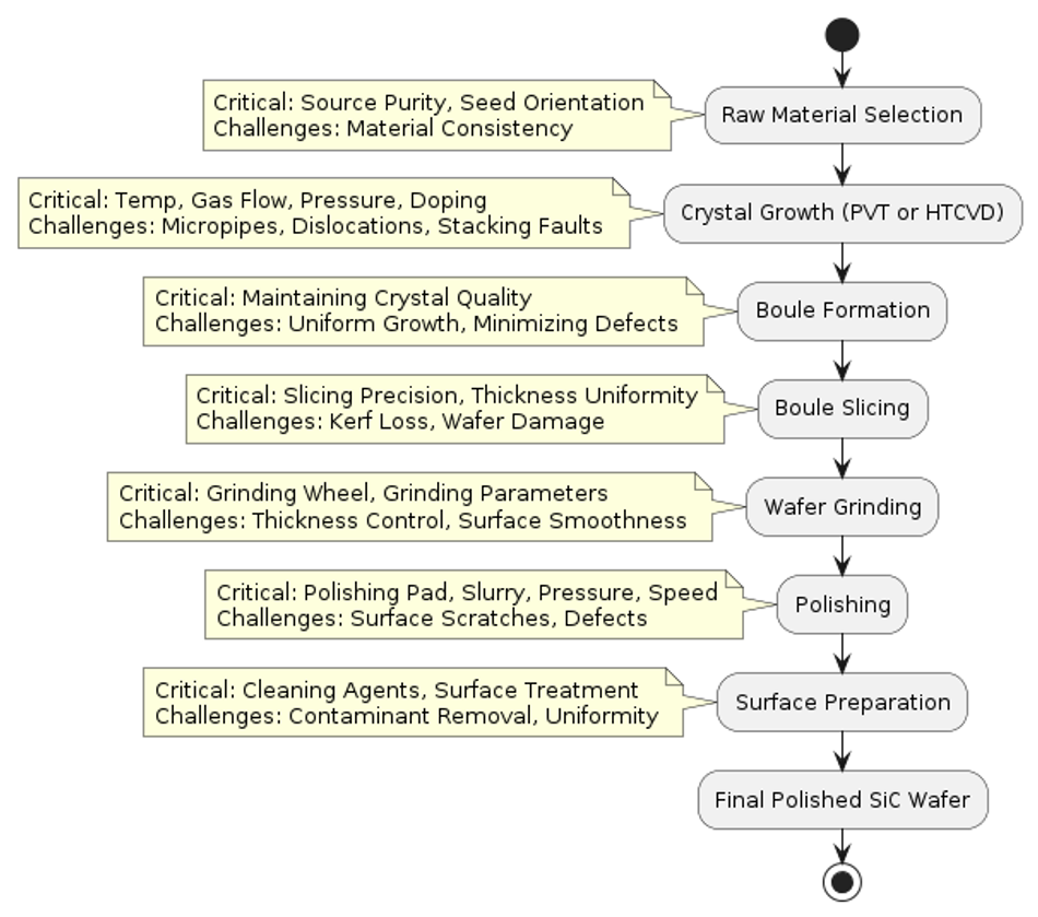
By mastering these techniques and overcoming the challenges of defect control, manufacturers pave the way for the creation of high-performance SiC wafers.
Advancements in SiC Wafer Technology
SiC wafer technology is on a relentless march forward, driven by exciting advancements:
Larger Wafers, Greater Efficiency: The availability of SiC wafers with larger diameters, reaching up to 150mm and even 200mm, is a game-changer. These larger wafers allow for increased device integration on a single chip, leading to higher production throughput and ultimately reduced manufacturing costs per unit area.
Taming Defects, Refining Quality: The relentless pursuit of reducing defects and improving crystal quality has spurred the development of advanced growth techniques. Techniques like Continuous Feed Physical Vapor Transport (CF-PVT) and refined High-Temperature Chemical Vapor Deposition (HTCVD) minimize defect densities and pave the way for exceptional SiC crystals.
State-of-the-Art Characteristics: Leading manufacturers are delivering SiC wafers with truly impressive characteristics. Low defect densities (often less than 10 micropipes per square centimeter) and high carrier lifetimes are hallmarks of these advanced wafers. This translates to the fabrication of high-performance SiC devices with superior efficiency and reliability.
Epitaxial Growth Takes Center Stage: Significant advancements in epitaxial growth techniques are contributing to the overall quality of SiC wafers. Cutting-edge methods like Chloride-Based Chemical Vapor Deposition (CVD) and Trichlorosilane (TCS) CVD offer unparalleled control over doping profiles, layer thickness, and defect densities within the epitaxial SiC layers.
Doping with Precision: Doping, the process of introducing impurities to control the electrical properties of SiC wafers, has become an art form. Techniques like ion implantation and in-situ doping during epitaxial growth have been meticulously refined, allowing for precise control over dopant concentrations and activation. Common dopants include nitrogen for n-type (electron-rich) and aluminum or boron for p-type (hole-rich) conductivity.
Seeing the Unseen: Advanced Characterization: The relentless pursuit of perfection extends to characterization techniques. Advanced methods like X-ray topography, photoluminescence mapping, and scanning electron microscopy (SEM) are used to not only identify defects but also analyze them in detail. This continuous monitoring allows manufacturers to refine their processes and steadily improve wafer quality, ultimately leading to even better device performance.
Technique | Chemical Vapor Deposition (CVD) | Molecular Beam Epitaxy (MBE) |
Growth Environment | Reactor Chamber | Ultra-High Vacuum |
Precursors | Gaseous (e.g., SiH4, C3H8) | Elemental Sources |
Growth Temperature | 1500-1800°C | 1000-1500°C |
Growth Rate | High | Low |
Doping Control | Good | Excellent |
Scalability | High | Low |
Applications | Commercial Production | Research, Specialized Devices |
Recommended reading: Understanding the Difference Between Wafers and Chips in Semiconductor Manufacturing
Applications of SiC Wafers in Engineering
Silicon Carbide (SiC) wafers have emerged as a game-changer in the engineering landscape, particularly within power electronics and radio frequency (RF) applications. Their exceptional properties, stemming from the wide bandgap, high breakdown electric field, and superior thermal conductivity, make them ideal for building high-performance, efficient devices.
Revolutionizing Power Electronics
SiC wafers have fundamentally transformed power electronics by enabling the development of advanced devices with unmatched performance:
Higher Voltages, Lower Losses: The wide bandgap of SiC allows operation at higher voltages, reducing energy wasted during switching events and leading to significant efficiency gains.
Compact Designs, Cooler Operation: The high thermal conductivity of SiC efficiently dissipates heat, enabling the creation of compact and lightweight power conversion systems without the need for bulky cooling solutions.
These advantages translate into tangible benefits across various sectors:
Electric Vehicles (EVs): SiC-based traction inverters and on-board chargers contribute to longer driving ranges and faster charging times for EVs by improving power conversion efficiency.
Renewable Energy Systems: SiC devices in solar inverters and wind turbine converters enable more efficient conversion and integration of renewable energy sources into the power grid.
Industrial Motor Drives: SiC-based motor drives offer significant advantages, including higher efficiency, reduced energy consumption, and improved motor reliability in industrial applications.
High-Voltage Direct Current (HVDC) Transmission: SiC devices enable efficient long-distance transmission of electrical power with minimal energy losses.
Mastering the High-Frequency Domain
Beyond power electronics, SiC wafers are making waves in the world of RF and microwave devices:
Unmatched Power Handling: The high electron mobility of SiC allows for superior power handling capability compared to traditional silicon-based devices.
High-Frequency Operation at High Temperatures: The wide bandgap of SiC enables efficient operation at high frequencies and elevated temperatures, crucial for demanding applications.
These characteristics make SiC ideal for:
Power Amplifiers: SiC-based power amplifiers offer higher output power, improved efficiency, and better thermal management compared to silicon counterparts, finding applications in wireless communications, radar systems, and satellite communications.
Radar Systems: SiC technology allows for the development of high-performance radar systems with greater range and resolution due to their ability to handle high power levels and operate at high frequencies, benefiting both military and civilian applications.
Satellite Communications: SiC-based amplifiers and transceivers provide significant advantages in harsh space environments where high power and high-frequency operation are essential for reliable communication.
Wireless Infrastructure: SiC-based devices can unlock higher data rates and improved coverage in wireless infrastructure like base stations and cellular networks while maintaining high efficiency and reliability.
The potential applications of SiC wafers extend far beyond the examples listed here. As research and development efforts continue, we can expect to see SiC technology revolutionize even more sectors in the engineering field, shaping a future powered by efficiency, performance, and innovation.
Defect Control and Yield Improvement
While SiC wafers offer remarkable properties, they are not without their challenges. Defects like micropipes, dislocations, stacking faults, and impurities can act as gremlins, sabotaging device performance and reliability. These defects create unwanted pathways for electricity to flow, leading to:
Reduced Efficiency: Ideally, all current should flow through the intended channels in a device. Defects create leakage paths, diverting current and reducing overall efficiency.
Increased Leakage Currents: Leakage currents represent wasted energy, leading to higher operating temperatures and potential device failure.
Premature Device Failure: In severe cases, defects can cause devices to fail prematurely, impacting system reliability.
To combat these challenges, a multi-pronged approach is employed:
Crystal Growth Optimization: Since many defects originate during crystal growth (PVT or CVD), meticulous control of growth parameters is essential. Precise temperature gradients, gas flow rates, and impurity levels are crucial for minimizing defect formation from the very beginning.
Advanced Characterization Techniques: Early detection and identification of defects are paramount. Here's where sophisticated tools come into play:
X-ray Topography: This technique acts like an X-ray for defects, revealing their presence and distribution within the SiC wafer.
Photoluminescence Mapping: This method shines a light on defects, literally. By analyzing how light interacts with the wafer, engineers can identify defects and assess their impact on electrical and optical properties.
Scanning Electron Microscopy (SEM) and Transmission Electron Microscopy (TEM): These powerful microscopes provide a high-resolution view of the SiC wafer, allowing for detailed analysis of defects down to the nanoscale level.
Post-Growth Processing Techniques: Even after growth, efforts continue to minimize defects and improve yield:
High-Temperature Annealing: This process involves heating the SiC wafer to a high temperature, which can help to heal or reduce the severity of certain defects.
Epitaxial Growth of Buffer Layers: A defect-free layer of SiC can be grown on top of the initial wafer, essentially burying any defects and creating a pristine surface for device fabrication.
Surface Treatments: Techniques like Chemical-Mechanical Polishing (CMP) and Reactive Ion Etching (RIE) can be used to remove or smooth out surface defects, improving device performance.
By employing these strategies, manufacturers can significantly reduce defect densities and create high-quality SiC wafers, paving the way for the development of reliable and efficient SiC devices that push the boundaries of engineering.
Packaging and Integration Challenges
SiC devices boast impressive capabilities – high-temperature operation and exceptional power handling. However, these very strengths present unique challenges when it comes to packaging and integration. Here, two major hurdles come into focus: thermal management and interconnect reliability.
Thermal Management: A Balancing Act: SiC devices operate at high power densities, generating significant heat. Efficient heat dissipation is paramount to prevent device degradation and premature failure. Traditional packaging materials and techniques, often designed for cooler operating temperatures, may not suffice. Innovative solutions are needed to effectively transfer heat away from the device.
Interconnect Reliability: Under Pressure: The high operating temperatures and thermal cycling that SiC devices experience can put a strain on the interconnects, and the electrical pathways between the device and the package. This thermal stress can lead to mechanical fatigue and, ultimately, interconnect failures, jeopardizing system reliability. Careful material selection and design techniques are crucial to ensure robust interconnects that can withstand these demanding conditions.
Researchers are actively developing packaging solutions to address these challenges:
High-Temperature Ceramic Packages: Materials like aluminum nitride and silicon nitride offer a compelling combination of excellent thermal conductivity and the ability to withstand high temperatures, making them ideal candidates for SiC device packaging.
Metal Matrix Composite Packages: These innovative packages incorporate metal matrices reinforced with ceramic particles or fibers. This unique structure provides both the high thermal conductivity needed for heat dissipation and the mechanical strength required for reliable operation.
Double-Sided Cooling Packages: As the name suggests, these packages incorporate cooling solutions on both the top and bottom surfaces of the device. This double-barreled approach significantly enhances heat dissipation capabilities.
Advanced Interconnect Technologies: Researchers are exploring next-generation interconnect technologies such as:
Wire bonding with high-temperature materials: Utilizing wires made from materials that can handle the heat, ensuring reliable connections.
Flip-chip bonding: This technique creates a more direct connection between the device and the package, improving thermal performance and electrical performance.
Sintered silver interconnects: Silver sintered at high temperatures forms a strong and conductive connection between the device and the package.
Conclusion
Silicon carbide (SiC) wafers have emerged as a revolutionary material in power electronics, offering superior performance and efficiency compared to traditional silicon-based devices. Their unique properties, like wide bandgap, high breakdown electric field, and high thermal conductivity, have enabled advanced power electronic devices capable of operating at higher voltages, temperatures, and frequencies.
SiC-based devices are employed in renewable energy systems, electric vehicles, industrial motor drives, and high-voltage direct current (HVDC) transmission systems, offering improved efficiency, reduced power losses, and compact form factors.
The future development and adoption of SiC wafer technology are expected to accelerate, driven by ongoing research in crystal growth techniques, epitaxial growth methods, and packaging solutions, as well as the increasing demand for energy-efficient and high-power applications.
Frequently Asked Questions
Advantages of SiC wafers over silicon wafers?
Wide bandgap for higher voltage and temperature operation
High breakdown electric field for smaller device dimensions and higher power densities
High thermal conductivity for efficient heat dissipation
Common applications of SiC wafers?
Renewable energy systems (solar inverters, wind turbine converters)
Electric vehicle traction inverters and on-board chargers
Industrial motor drives and power converters
High-voltage direct current (HVDC) transmission systems
Aerospace and defense applications (radar systems, satellite communications)
How are SiC wafers produced?
Bulk SiC crystals are grown using techniques like PVT and CVD
Wafers sliced from grown SiC boules and undergo surface preparation
Challenges in SiC wafer production?
Controlling crystal defects like micropipes, dislocations, and stacking faults
Achieving high crystal quality and low defect densities
Developing advanced epitaxial growth techniques for precise doping control
Key considerations for packaging SiC devices?
Thermal management due to high power densities and operating temperatures
Interconnect reliability under high-temperature and thermal cycling conditions
Development of suitable packaging materials and techniques
References
X. She, A. Q. Huang, Ó. Lucía and B. Ozpineci, "Review of Silicon Carbide Power Devices and Their Applications," in IEEE Transactions on Industrial Electronics, vol. 64, no. 10, pp. 8193-8205, Oct. 2017, doi: 10.1109/TIE.2017.2652401.
S. Ji, Z. Zhang, and F. Wang, "Overview of high voltage sic power semiconductor devices: development and application," in CES Transactions on Electrical Machines and Systems, vol. 1, no. 3, pp. 254-264, September 2017, doi: 10.23919/TEMS.2017.8086104.
B. J. Baliga, "Silicon Carbide Power Devices: Progress and Future Outlook," in IEEE Journal of Emerging and Selected Topics in Power Electronics, vol. 11, no. 3, pp. 2400-2411, June 2023, doi: 10.1109/JESTPE.2023.3258344.
A. K. Agarwal et al., "SiC electronics," International Electron Devices Meeting. Technical Digest, San Francisco, CA, USA, 1996, pp. 225-230, doi: 10.1109/IEDM.1996.553573.
Das, Hrishikesh & Sunkari, Swapna & Justice, Joshua & Pham, Helen & Park, Kyeong. (2019). Effect of Defects in Silicon Carbide Epitaxial Layers on Yield and Reliability. Materials Science Forum. 963. 284-287. 10.4028/www.scientific.net/MSF.963.284.
Seal S, Mantooth HA. High-Performance Silicon Carbide Power Packaging—Past Trends, Present Practices, and Future Directions. Energies. 2017; 10(3):341. https://doi.org/10.3390/en10030341