QFN Packages: A Guide to High-Performance Electronics Encapsulation
The Quad Flat No-leads (QFN) package is a type of surface-mount technology (SMT) in the electronics industry known for its compact size and high performance. This comprehensive guide explores its benefits (high performance), applications (mobile devices), and challenges (assembly, soldering).

21 Feb, 2024. 14 minutes read
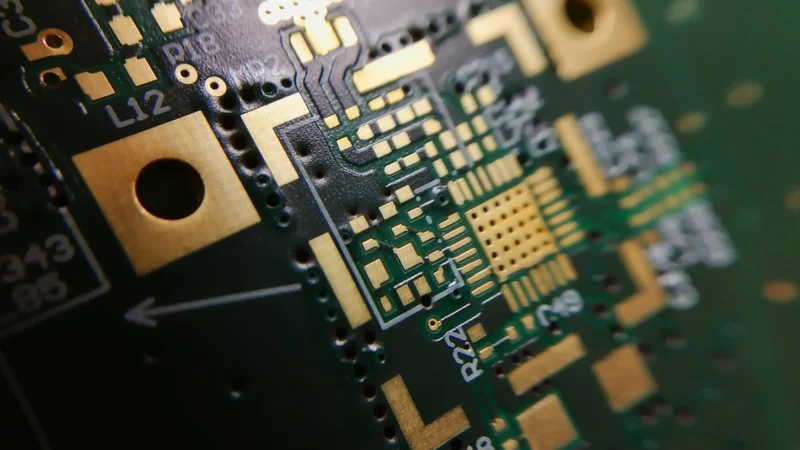
QFN (quad flat no-leads) technology footprint on PCB
Introduction to QFN Package
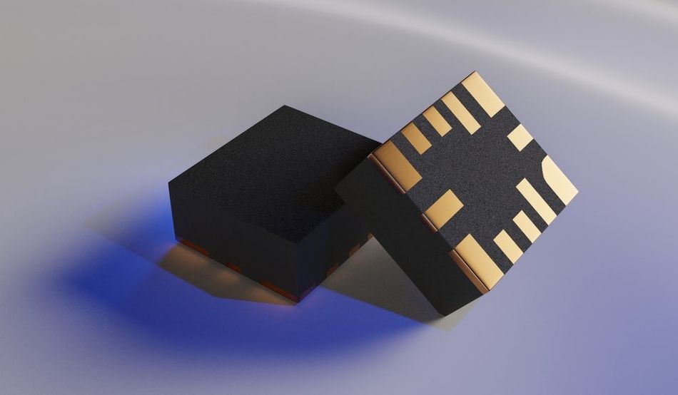
The Quad Flat No-leads (QFN) package, a prominent semiconductor surface-mount technology, is revered for its compactness and superior performance in the electronics industry. This leadless package, with an exposed pad for enhanced thermal dissipation, is a favored choice for high-density applications owing to its diminutive footprint and slender profile. Crafted as a near-chip scale plastic-encapsulated entity, it boasts a copper lead frame substrate meticulously designed to establish electrical connections to the integrated circuit (IC).
Meanwhile, the plastic body serves the dual purpose of shielding the IC and dispersing heat generated during operation, ensuring optimal performance. Distinguishing itself with its innovative 'no leads' design, the quad flat no-lead package eschews traditional protruding leads, opting for bottom-mounted terminal pads instead. These pads, seamlessly soldered onto the printed circuit board (PCB), optimize spatial efficiency and enhance electrical performance.
Widely deployed across mobile devices, automotive electronics, and high-speed data processing systems, the QFN package's compactness, high performance, and cost-effectiveness make it a preferred solution for discerning electronic design engineers. Nonetheless, its adoption comes with inherent challenges, including meticulous attention to the assembly process and adept handling of soldering intricacies, necessitating thorough consideration throughout the design and manufacturing phases.[1]
The Basics of QFN Package
The Quad Flat No-leads (QFN) package emerges as a cornerstone of surface-mount technology in the electronics realm, lauded for its compactness, high performance, and cost-effectiveness. This innovative packaging solution epitomizes efficiency, resembling a near-chip scale plastic-encapsulated marvel underpinned by a copper lead frame substrate.
Engineered with precision, the QFN package melds a copper lead frame to facilitate electrical interconnection with the integrated circuit (IC). At the same time, a durable plastic body safeguards the IC and dissipates heat during operation. A hallmark of QFN's ingenuity lies in its 'no leads' design, which eschews conventional protruding leads in favor of bottom-mounted terminal pads. These thermal pads, seamlessly integrated into the PCB design, optimize spatial utilization and augment electrical performance.
The QFN package's versatility extends beyond traditional IC packaging methods, embracing modern techniques such as BGA (Ball Grid Array), die-attach, flip chip technology, and interconnection, ensuring it remains at the forefront of innovation in the ever-evolving electronics landscape. As a leading player in IC packaging, QFN has established itself as a formidable contender alongside other packaging formats like QFP (Quad Flat Package), ushering in a new era of miniaturization and performance optimization.[2]
Further reading: Types of IC Packages: A Comprehensive Guide
Components of a QFN Package
The QFN package comprises several vital components essential to its operation. The integrated circuit (IC) is the core functional unit, typically housing thousands or millions of transistors responsible for processing tasks.
The second crucial component is the lead frame, a thin copper layer facilitating electrical connections between the IC and external circuitry. Configured with leads or traces corresponding to the IC's input and output pins, the lead frame links to terminal pads on the package's underside and is subsequently soldered onto the PCB.
In addition to the lead frame, wire bonding plays a significant role in establishing connections within the QFN package. Wire bonding involves connecting the IC to the lead frame using fine wires, ensuring electrical conductivity and signal transmission between components.
Moreover, the plastic body provides mechanical support and aids in thermal dissipation for the IC. Crafted from thermally conductive materials, it efficiently disperses heat generated during operation, which is crucial for high-performance applications where heat management is paramount.
Finally, the terminal pads on the package's underside, directly soldered onto the PCB, furnish secure and reliable electrical connections. Their location optimizes space utilization by eliminating side protrusions, enhancing electrical performance through minimized lead lengths, reduced signal delay, and improved signal integrity.
Varieties of QFN Packages
The QFN package encompasses various types tailored to specific application needs, including the standard QFN, thin QFN (TQFN), micro QFN (MQFN), and the innovative air-cavity QFN.
The standard QFN, prevalent across diverse applications, features a square or rectangular shape with terminal pads on the bottom. Renowned for its compact size, high performance, and cost-effectiveness, the standard QFN remains a staple in electronics design.
In contrast, the TQFN offers a slimmer profile catering to applications where height is crucial. Sharing the basic structure of the standard QFN, the TQFN distinguishes itself with a thinner plastic body, ideal for slim devices like smartphones and tablets.
Similarly, the MQFN serves applications prioritizing space efficiency, boasting a smaller footprint than its standard counterpart. Tailored for high-density environments such as wearable devices and Internet of Things (IoT) devices, the MQFN optimizes space utilization without compromising performance.
Introducing the air-cavity QFN, this innovative variant incorporates an air gap within the package, enhancing thermal dissipation and reducing the risk of thermal stress on sensitive components. The air-cavity design also mitigates the effects of moisture, ensuring long-term reliability in challenging environmental conditions.
Each quad flat no-lead package type presents distinct advantages and limitations, guiding the selection process based on specific application requirements. While the standard QFN excels in general-purpose applications, the TQFN or MQFN may be preferred for space or height-constrained designs.
Meanwhile, the air-cavity QFN offers enhanced thermal management, making it suitable for applications demanding superior heat dissipation and reliability.
Further reading: QFN and aQFN options for the nRF52840
The Working Principle of QFN Package
The QFN package provides a reliable and efficient electrical connection between the integrated circuit (IC) and the printed circuit board (PCB). The IC, the package's primary functional unit, is mounted on a copper lead frame. The lead frame serves as a conduit for electrical signals, routing them from the IC to the terminal pads on the bottom of the package. These terminal pads are soldered directly onto the PCB, ensuring a secure and reliable electrical connection.
The 'no leads' design of the QFN package contributes to its high performance. The package can achieve shorter lead lengths by eliminating the need for protruding leads, reducing signal delay, and increasing signal integrity. This is particularly important in high-speed applications, where signal integrity is critical for proper functioning.[3]
Heat Dissipation in QFN Packages
One of the key features of the QFN package is its ability to dissipate heat effectively. The plastic body of the package is typically made of a thermally conductive material, which helps to transfer heat generated by the IC away from the package during operation. This is crucial for maintaining the performance and reliability of the IC, as excessive heat can lead to degradation and failure.
Several factors facilitate the heat dissipation process in a QFN package. First, the copper lead frame, an excellent conductor of heat, helps spread the heat generated by the IC across the package. Second, the terminal pads on the bottom of the package provide a direct thermal path to the PCB, allowing heat to be transferred to the board and dissipated into the surrounding environment.
In some cases, additional heat dissipation techniques may be employed further to enhance the thermal performance of the QFN package. These can include thermal vias in the PCB, which provide a direct path for heat to flow from the package to the board's ground plane, or incorporate a heat sink or other cooling solution to help dissipate heat more effectively.
Electrical Performance of QFN Packages
The QFN package's electrical performance, characterized by its low inductance, is a cornerstone of its appeal, making it a top choice for numerous high-speed and high-frequency applications. Its innovative 'no leads' design significantly bolsters this aspect, paving the way for superior electrical efficiency.
This stellar performance is achieved through several key mechanisms. Firstly, eliminating protruding leads enables the package to establish shorter signal paths, thereby minimizing signal delay and enhancing signal integrity—a critical factor in high-speed scenarios where precision is paramount.
Furthermore, the copper lead frame within the QFN package is pivotal in enhancing its electrical capabilities. Leveraging copper's excellent conductivity, the lead frame facilitates a low-inductance pathway for electrical signals, ensuring a robust and efficient connection from the integrated circuit (IC) to the terminal pads. This seamless connectivity is indispensable for the IC's optimal operation.
Moreover, terminal pads on the bottom of the QFN package foster a direct electrical linkage to the printed circuit board (PCB) and augment its electrical performance. This configuration guarantees a secure and reliable connection. It optimizes space utilization by eliminating side protrusions, reducing signal delay, and bolstering signal integrity—a boon for demanding high-speed applications.
In addition to its stellar electrical prowess, the QFN package also excels in thermal performance. Crafted from thermally conductive materials, its plastic body efficiently dissipates heat generated by the IC during operation, safeguarding against performance degradation and potential failure—a testament to its holistic design and engineering prowess.
Advantages of QFN Packages
The QFN package stands out for its compact size and high performance, making it a favored option in various electronic applications. Its 'no leads' design optimizes space utilization, which is particularly advantageous for high-density scenarios. With a small footprint and thin profile, the QFN package is well-suited for compact devices like smartphones, tablets, and wearable technology.
In addition to the Quad Flat No-leads (QFN) package, the electronics industry also benefits from the Chip Scale Package (CSP), which provides unique advantages in terms of miniaturization and performance optimization.
Similarly, the CSP, known for its minimal footprint and high performance, further advances miniaturization efforts in electronic design. By eliminating the need for traditional packaging components such as leads or external connectors, the CSP achieves exceptional space efficiency, which is ideal for modern devices requiring compact form factors without compromising performance.
Furthermore, the QFN package offers outstanding electrical performance, with its short lead lengths minimizing signal delay and improving signal integrity. This feature makes the QFN package suitable for high-speed and high-frequency applications. Additionally, the copper lead frame within the QFN package ensures a reliable and efficient electrical connection, further enhancing its performance capabilities.
Moreover, both the QFN and CSP packages excel in thermal management. The QFN's thermally conductive plastic body effectively dissipates heat generated by the integrated circuit during operation, which is crucial for maintaining optimal performance and reliability. Similarly, the CSP's compact design allows for efficient heat dissipation, ensuring stable operation and longevity of electronic components.[4]
Size and Weight Benefits
One of the key advantages of the QFN package is its size and weight benefits. The QFN package is significantly smaller and lighter than traditional packages with protruding leads. This makes it an ideal choice for compact devices where space and weight are critical factors.
The compact size of the QFN package is largely due to its 'no leads' design. The package can achieve a smaller footprint and a thinner profile by eliminating the need for protruding leads. This not only reduces the overall size of the package but also allows for a more efficient use of space on the PCB.
The weight of the QFN package is also significantly less than that of traditional packages. A thin copper lead frame and a lightweight plastic body result in a lighter package that is more suitable for portable devices. This can be particularly beneficial in wearable devices and mobile electronics applications, where weight is critical.
Performance Benefits
The QFN package offers several performance benefits, making it a popular choice for many applications. One key benefit is its excellent electrical performance. The short lead lengths in the QFN package reduce signal delay and increase signal integrity, making it suitable for high-speed and high-frequency applications. The copper lead frame provides a low-resistance path for electrical signals, ensuring a reliable and efficient electrical connection.
Another significant performance benefit of the QFN package is its superior thermal performance. The plastic body of the package is typically made of a thermally conductive material, which helps to dissipate heat generated by the IC during operation. This is crucial for maintaining the IC's performance and reliability, as excessive heat can lead to degradation and failure.
The 'no leads' design of the QFN package also contributes to its high performance. The package can achieve shorter lead lengths by eliminating the need for protruding leads, reducing signal delay, and increasing signal integrity. This is particularly important in high-speed applications, where signal integrity is critical for proper functioning.
The QFN package also offers good mechanical performance. Its plastic body provides mechanical support to the IC, protecting it from physical stress and damage. The package's small footprint and thin profile also make it an ideal choice for compact devices, where mechanical robustness is critical.
Challenges with QFN Packages
Despite the numerous advantages of QFN packages, they also present certain challenges that must be considered during design and manufacturing. These challenges primarily revolve around assembly, soldering, inspection, and testing.[5]
Assembly and Soldering Challenges
The 'no leads' configuration intrinsic to QFN packages presents unique challenges during assembly and soldering compared to traditional packages with protruding leads, potentially affecting IPC (Institute for Printed Circuits) standards. Achieving precise alignment of the terminal pads on the package with those on the printed circuit board (PCB) proves challenging due to the pads' small size and strict tolerances.
Furthermore, soldering QFN packages demands precision, particularly with the bottom terminal pads. These require carefully controlled amounts of solder paste to ensure reliable electrical connections. Inadequate solder paste may result in weak or absent connections, while excessive paste can lead to solder bridging or short circuits between adjacent pads.
Designers and manufacturers must meticulously plan the assembly and soldering processes to address these challenges and comply with IPC standards. This includes implementing appropriate solder paste stencils and stencil designs, precise placement equipment, and optimizing reflow soldering profiles to guarantee the integrity and reliability of the solder joints. Additionally, considerations such as pad design, solder mask application, wettable flanks, and rework procedures must be carefully integrated into the assembly workflow to ensure consistent and high-quality outcomes.
Further reading: Demystifying Soldering Techniques: A Comparison of Wave Soldering and Reflow Soldering
Inspection and Testing Challenges
Inspecting and testing QFN packages present unique challenges due to their 'no leads' design. Traditional packages with protruding leads can be easily inspected visually or using automated optical inspection (AOI) systems to check for soldering defects. However, the bottom terminal pads of QFN packages are not easily visible, making it difficult to inspect the solder joints directly.
This lack of visibility can make detecting and rectifying defects such as insufficient solder, excessive solder, or misaligned components challenging. These defects can lead to poor electrical connections, affecting the IC's performance and reliability.
To overcome these challenges, manufacturers may rely on alternative inspection methods like X-ray or electrical testing. X-ray inspection can provide a detailed view of the solder joints, allowing for the detection of defects that are not visible to the naked eye. On the other hand, electrical testing can verify the IC's functionality and the electrical connections' integrity.
Despite these challenges, the benefits of QFN packages often outweigh the difficulties. The QFN package can provide a compact, high-performance solution for various applications with careful design, precise assembly, and thorough inspection and testing.
Applications of QFN Packages
The Quad Flat No-leads (QFN) package, a Surface Mount Device (SMD), is widely favored across various industries for its compact size, high performance, and impressive thermal and electrical characteristics. This versatile package finds applications in mobile devices, automotive electronics, and high-speed data processing systems.
Renowned for its small footprint and slender profile, the QFN package is ideal for compact devices with limited space. Its compact size and excellent electrical performance, including reduced signal delay and increased signal integrity, make it well-suited for high-speed and high-frequency applications. Moreover, the package's efficient thermal performance, facilitated by the thermally conductive material of the plastic body, is invaluable in applications where effective heat dissipation is paramount.
Furthermore, the QFN package is available in various sizes and pin counts, catering to diverse application needs. Its punch-type design and compatibility with Dual Flat No-leads (DFN) packages offer flexibility in design and assembly, allowing efficient integration into a wide range of electronic systems.[6]
Use in Mobile Devices
One of the primary applications of QFN packages is in mobile devices such as smartphones, tablets, and wearable devices. The compact size and lightweight nature of the QFN package make it an ideal choice for these devices, where space and weight are critical factors.
In mobile devices, QFN packages are often used to package integrated circuits (ICs) that perform various functions, including processing, memory, power management, and wireless communication. The QFN package's high-speed and high-frequency performance is particularly beneficial in these applications, as it supports modern mobile devices' high data rates and fast processing speeds.
The QFN package's good thermal performance is also crucial in mobile devices, as these devices often generate significant amounts of heat due to their high processing speeds and power densities. The ability of the QFN package to effectively dissipate this heat helps to maintain the performance and reliability of the ICs, thereby contributing to the overall performance and user experience of the mobile device.
Use in Automotive Electronics
The automotive industry is another significant area where QFN packages find extensive application. Modern vehicles increasingly rely on electronics for various functions, including engine control, infotainment systems, safety features, and driver assistance systems. The QFN package, compact size, excellent electrical performance, and good thermal characteristics, is well-suited to meet the demands of these applications.
In engine control, QFN-packaged ICs are often used in electronic control units (ECUs) that manage various aspects of the vehicle's engine, such as fuel injection, ignition timing, and emission control. The high-speed and high-frequency performance of the QFN package is crucial in these applications, as it enables the rapid processing of sensor data and the timely execution of control commands.
Infotainment systems in vehicles, including audio and video playback, navigation, and connectivity features, also benefit from using QFN packages. The compact size of the QFN package allows for integrating many functions into a small space. At the same time, its excellent electrical performance supports the high data rates required for audio and video streaming.
Safety features and driver assistance systems, such as anti-lock braking systems (ABS), electronic stability control (ESC), and advanced driver-assistance systems (ADAS), are other areas where QFN packages are used. These systems often require the processing of large amounts of data in real time, which is facilitated by the high-speed performance of the QFN package.
The thermal performance of the QFN package is also a key factor in automotive applications. Vehicles can operate in various temperatures, and their electronics must withstand these conditions. The ability of the QFN package to effectively dissipate heat helps to maintain the performance and reliability of the ICs, even under harsh operating conditions.
Conclusion
The Quad Flat No-leads (QFN) package is a highly versatile and efficient packaging technology widely used in various industries, including mobile devices and automotive electronics. Its compact size, excellent electrical and thermal performance, and cost-effectiveness make it an attractive choice for many applications. However, it also presents certain challenges, particularly regarding assembly, soldering, inspection, and testing. Despite these challenges, with careful design, precise assembly, and thorough inspection and testing, the QFN package can provide a compact, high-performance solution for various applications.
FAQs
What is a QFN package?
A QFN (Quad Flat No-leads) package is a type of surface-mount technology (SMT) package used to house integrated circuits (ICs). It is characterized by its small size, thin profile, and 'no leads' design, with terminal pads located on the bottom of the package.
Why is the QFN package widely used?
The QFN package is widely used due to its compact size, excellent electrical and thermal performance, and cost-effectiveness. Its small footprint and thin profile make it an ideal choice for compact devices where space is at a premium. Its excellent electrical performance, including reduced signal delay and increased signal integrity, makes it suitable for high-speed and high-frequency applications. The package's good thermal performance is facilitated by the thermally conductive material of the plastic body, which is crucial in applications where heat dissipation is a key concern.
What are the challenges associated with using QFN packages?
The main challenges of using QFN packages revolve around assembly, soldering, inspection, and testing. The 'no leads' design can make assembly and soldering more difficult than traditional packages with protruding leads. The bottom terminal pads of QFN packages are not easily visible, making it difficult to inspect the solder joints directly. To overcome these challenges, manufacturers may rely on alternative inspection methods like X-ray or electrical testing.
What are some applications of QFN packages?
QFN packages are used in a variety of applications across different industries. They are commonly used in mobile devices such as smartphones, tablets, and wearable devices, where their compact size and lightweight nature are beneficial. In the automotive industry, QFN packages are used in electronic control units (ECUs) that manage various aspects of a vehicle's engine and infotainment systems, safety features, and driver assistance systems.
Reference
J. Lee and S. Kang (2012). Quad Flat No-Lead (QFN) Package Development for High-Performance and High-Density Applications. IEEE Transactions on Components, Packaging, and Manufacturing Technology, 2(1), pp. 129-136.
UTmel Blog, 2021: Introduction to QFN Package. Available at: https://www.utmel.com/blog/categories/integrated%20circuit/the-introduction-to-qfn-package (Accessed: February 7, 2024).
RAYPCB, 2023. The Fundamental Analysis of QFP vs QFN Packages. Available at: https://www.raypcb.com/qfp-vs-qfn-packages/ (Accessed: February 7, 2024).
Cadence Design Systems, Inc., 2023. Available at: https://resources.pcb.cadence.com/blog/2023-qfn-package-process-flow-advantages-and-types (Accessed: February 7, 2024).
Aim Solder, 2024. Overcoming the Challenges of the QFN. Available at: https://aimsolder.com/technical-articles/overcoming-challenges-qfn (Accessed: February 8, 2024).
Microchip, 2019. Package Application Note for QFN and DFN Packages. Available at: https://www.farnell.com/datasheets/2076320.pdf (Accessed: February 8, 2024).