PNP Transistor: Theory, Operation and Practical Applications for Engineers
This article focuses on the PNP transistor, exploring its structure, physics, operating modes, differences from its NPN counterpart, and how to design reliable switching, amplification, and power management circuits using it.

16 Feb, 2026. 15 minutes read
Key Takeaways
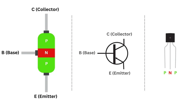
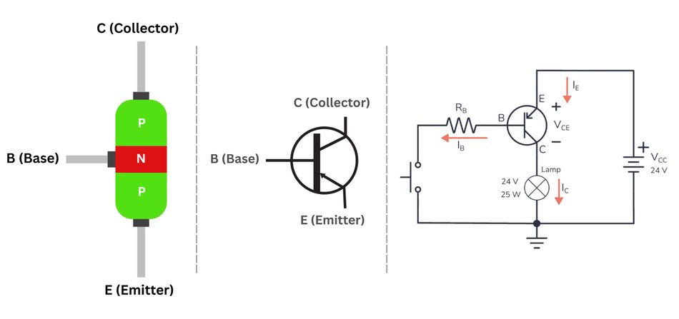
PNP transistor is a bipolar junction transistor where the majority charge carriers are holes. The emitter and collector regions are made of p‑type material, and the base is n‑type. Current flows from the emitter to the collector when the base‑emitter junction is forward-biased.
Biasing is opposite to an NPN device: to turn a PNP transistor on, the base must be pulled lower than the emitter; to turn it off, the base is brought close to the emitter potential. This polarity reversal is essential in designing high‑side switches and complementary amplifier stages.
PNP transistors excel at sourcing current. They are used in high‑side switching, complementary class‑B and class‑AB amplifiers, low‑dropout regulators and high‑side current mirrors.
The common-emitter configuration is less intuitive in PNP devices because the emitter is tied to a positive supply rather than ground. Design calculations for base resistors, saturation voltage and current gain still follow the same principles used for NPN devices.
Practical design requires consideration of datasheet parameters such as DC current gain, saturation voltage, base‑emitter voltage, and maximum collector current. For instance, the small‑signal 2N3906 has a β of around 60–300 and a low saturation voltage of around 0.25–0.4 V, while the power PNP TIP2955 can handle 15 A with a β of 20–70.
Introduction
Bipolar junction transistors (BJTs) are fundamental building blocks in electronics. Two polarities exist, NPN and PNP, named after the arrangement of semiconductor doping. Despite field‑effect devices dominating modern digital logic, BJTs remain indispensable in analog design, power management and interfacing. This article focuses on the PNP transistor, exploring its structure, physics, operating modes and real‑world applications.
For engineers who work with digital logic, microcontrollers, power supplies or analog circuits, understanding PNP transistors unlocks design options such as high‑side switches, complementary push–pull stages, low‑dropout (LDO) regulators and current mirrors. The following sections balance theory and practical guidance, discussing doping profiles, carrier flow, biasing equations, typical data‑sheet values, design procedures and application circuits. Throughout the article, comparative insights highlight how PNP devices differ from their more familiar NPN counterparts. By the end, you will be able to select and implement PNP transistors confidently in your hardware designs.
Basics of Bipolar Junction Transistors (BJTs)
Semiconductor Structure and Doping
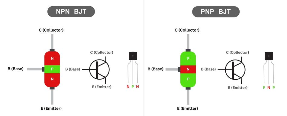
The bipolar junction transistor consists of two p–n junctions forming three regions: the emitter, base and collector.
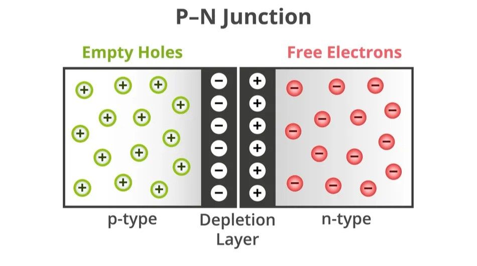
In a PNP transistor, the emitter and collector are p‑type, while the base is n‑type. The emitter is heavily doped to inject majority carriers; the base is very thin and lightly doped to permit most injected carriers to cross without recombination; the collector is moderately doped and larger to dissipate heat. The depletion region extends mainly into the lightly doped base, so the electric field across the collector–base junction helps sweep carriers out of the base.
The doping asymmetry serves two key purposes. First, heavy doping in the emitter ensures high injection efficiency: most carriers crossing the emitter–base junction originate from the emitter rather than the base. Second, the lightly doped, thin base reduces the likelihood that carriers recombine before reaching the collector. These characteristics yield a common‑base current gain (α) near unity and a common‑emitter current gain (β) typically between 50 and 300 for small‑signal devices. [1]
In PNP transistors, the majority carriers are holes, which have lower mobility than electrons. This results in slightly lower frequency performance than equivalent NPN devices. The emitter must be about 0.6 V above the base to forward bias the base–emitter junction, current flows out of the collector and the common‑emitter node is tied to the positive rail. These polarity reversals underlie the design differences explored later.
Charge Transport and Basic Operation
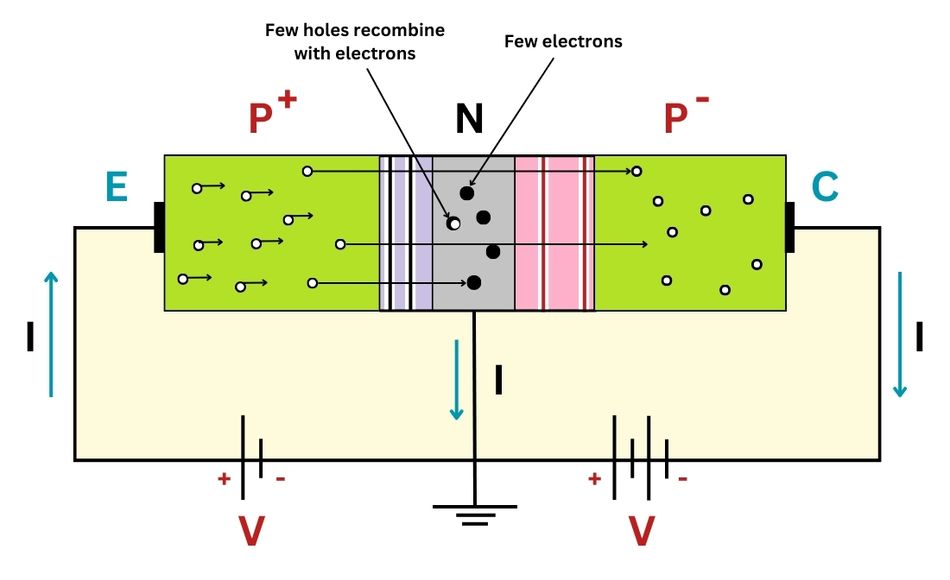
Once the emitter-base junction of a PNP transistor is forward-biased, holes are injected from the emitter into the base. Because the base is thin and lightly doped, only a fraction recombines; the majority traverse the base and are swept into the collector by the electric field across the reverse-biased base-collector junction. Resultantly, the collector current closely follows the emitter current, while the base current remains relatively small and flows in opposite directions to conventional NPN current paths.
This operating principle explains how a transistor works as a current-controlled device: a small base current governs a larger collector current, enabling amplification in analog amplifier circuits measured in amps or milliamps. In the active region, the relationship is defined by:

where β represents the DC current gain. The voltage behavior across the device, including VCE, determines whether the transistor operates in active, cut-off, or saturation mode. These characteristics directly influence impedance, signal swing, and performance in practical transistor circuits, topics commonly addressed in advanced tutorials and design references.
Recommended Reading: N-Type Vs P-Type: Difference Between P-Type and N-Type Semiconductors
Biasing and Operating Regions
The transistor can operate in four regions: cut‑off, active, saturation, and reverse active. Understanding these modes is essential for switching and amplifier design.
Cut‑Off (Off State)
In the cut‑off, both junctions are reverse-biased. For a PNP device, the emitter potential is more negative than the base potential. With no base current, the collector current drops to zero, and the transistor behaves like an open switch. Designers should ensure that the base–emitter voltage stays below about −0.5 V to avoid leakage. [2] When using PNP devices as high‑side switches, tie the base to the emitter via a resistor to pull the transistor off.
Active Region
The active region is used for amplification. The base–emitter junction is forward-biased, and the collector–base junction is reverse-biased. The PNP transistor conducts current from emitter to collector proportional to the base current. The relationship:

defines this mode, where β (or hFE) is the DC current gain specified in device datasheets. In small‑signal PNP devices, β may vary from ~60 to over 300, whereas power transistors like the TIP2955 exhibit β between 20 and 70 at high currents. Designers must account for variation across temperature and between devices by using minimum guaranteed β values in calculations.
Saturation (On State)
In saturation, both junctions are forward-biased. The base is driven sufficiently below the emitter such that the transistor conducts maximum current. In this mode, the collector–emitter voltage (VCE) drops to a low value, and the transistor functions as a closed switch. To guarantee saturation, the base current must exceed the collector current divided by a forced gain, typically 10–20. Due to hole mobility limitations in p-type semiconductor material, PNP devices exhibit slightly higher saturation voltages than NPN counterparts, especially in power transistors.
Reverse Active
This region occurs when the polarity of voltages is reversed such that the base–collector junction is forward-biased and the base–emitter junction is reverse-biased. It is rarely used intentionally because the current gain is very low and the breakdown risk is higher. A PNP transistor in reverse active behaves like an NPN with reversed terminals.
Voltage Relations Summary
Using conventional current direction, a PNP transistor operates correctly when voltage polarities are maintained in the proper order. In active mode, the emitter is at a higher potential than the base, which is higher than the collector. In saturation, both the collector and emitter are higher than the base. Reversing these relations places the device in a cutoff. [3] Understanding these polarity rules simplifies analysis when translating NPN schematic designs to PNP implementations.
Recommended Reading: How Does a Transistor Work? Theory & Practical Applications for Engineers
PNP Transistor as a Switch
Switching is one of the most common uses for BJTs. When acting as a digital switch, the transistor operates either in cut‑off or saturation. In digital logic or microcontroller interfacing, PNP transistors typically serve as high‑side switches: they connect the load to the positive supply rather than to ground.
High‑Side Switching Concept
In order to use a PNP transistor as a switch, the load is connected between the collector and ground, and the emitter is tied to the positive supply. To turn the switch on, the base is pulled to ground, forward-biasing the base–emitter junction. When the base is pulled up near the emitter potential, the transistor turns off. The base resistor limits the base current and protects the driving logic. The same equations for base resistor sizing, collector current and saturation as for NPN switches apply; only the polarities change.
Example: The small signal PNP device, such as the 2N3906, can control a 12 V lamp from a microcontroller. The emitter is tied to +12 V, the collector connects to the lamp, and the lamp’s other terminal is grounded. Driving the base low turns the switch on; driving it high turns it off. Because many controllers cannot tolerate voltages above their own supply, circuit designs often include level shifters, driver stages, or opto-isolators. If the control signal cannot reach the emitter potential, the transistor may not fully turn off, leading to leakage.
Base Resistor Calculation
Base resistor selection follows the same methodology used for NPN devices. For a required load current, choose a forced gain lower than the minimum guaranteed DC current gain to ensure saturation. The required base current is:
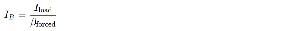
The base resistor value is then:
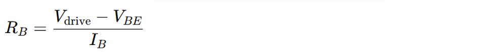
where V (drive) is the control voltage amplitude (0 V when turning on) and V (BE) is about 0.7 V for PNP silicon devices. In high‑side applications, the base often swings between the supply voltage and ground; thus, the resistor must be sized to ensure the base–emitter junction sees sufficient forward bias when the input is low but is not driven beyond the maximum base current when the input is high.
Protecting the Transistor
Switching inductive loads, such as relays or motors, requires a flyback diode across the load to absorb the back‑EMF when the transistor turns off.
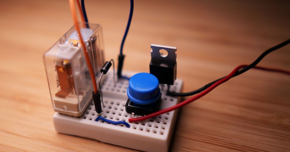
For PNP high‑side switches, the diode is connected from the emitter (positive supply) to the collector (load) with the cathode at the emitter. Additional protection, such as base–emitter resistors to discharge stored charge quickly, may improve turn‑off speed. When switching large currents or voltages, Darlington pairs or MOSFET drivers can provide the necessary current gain.
Recommended Reading: Transistor as a Switch: Theory and Practical Implementation for Digital and Hardware Engineers
Amplifier Circuits using PNP Transistors
Complementary Push–Pull Stages
Class‑B and class‑AB amplifiers use a pair of complementary transistors (one NPN and one PNP) to amplify opposite halves of an AC waveform. In a push‑pull configuration, the NPN amplifies the positive half of the waveform while the PNP amplifies the negative half. Each transistor conducts for approximately 180° of the signal’s cycle, and the outputs are combined to produce a continuous waveform. Complementary pairs reduce crossover distortion and improve efficiency compared with single‑ended amplifiers. Power amplifier designs often use matched pairs such as the TIP3055 (NPN) and TIP2955 (PNP) to deliver tens of amperes to loudspeakers or motors.
Small‑Signal Amplifier Stages
In discrete designs, PNP transistors are often used as active loads or current sources in differential pairs. For example, the input stage of an operational amplifier may use an NPN differential pair biased by a PNP current mirror, improving common‑mode rejection and maximizing output swing. In class‑A amplifiers, PNP devices can serve as constant current sources (current mirrors) to set bias currents. Their ability to source current from the positive rail makes them suitable for high‑side active loads, complementing NPN devices, which sink current to ground.
Gain and Frequency Considerations
The achievable voltage gain and bandwidth of a PNP-based amplifier are constrained by DC current gain, internal capacitances, and carrier mobility within the semiconductor material. Small-signal PNP devices such as the 2N3906 typically exhibit β values between 60 and 300 with transition frequencies on the order of hundreds of megahertz. In contrast, power transistors like the TIP2955 exhibit much lower β and a lower unity-gain frequency due to larger junction areas and increased charge storage.
Because holes in a p-type semiconductor have lower mobility than electrons in an n-type semiconductor, PNP transistors generally show lower high-frequency performance than comparable NPN devices. Designers can mitigate these effects with circuit techniques such as emitter degeneration, feedback, and compensation.
Recommended Reading: Understanding NPN vs PNP Transistors: A Comprehensive Guide
Current Mirrors and Active Loads
Principles of the Current Mirror
The current mirror is a fundamental transistor circuit that replicates a reference current with high accuracy, independent of load resistance. In its simplest bipolar implementation, two matched BJTs are used. One transistor is configured as a diode by shorting its base-collector junction, forcing the device into a defined operating point. The resulting base-emitter voltage establishes a reference that biases the second transistor. Provided both devices share the same semiconductor material, geometry, and temperature, the collector current of the output transistor closely matches the reference current.
In practice, mirror accuracy is limited by finite DC current gain, device mismatch, and non-ideal output impedance. Because each transistor draws a small current at the base, the mirrored current is slightly reduced. This error becomes more pronounced at low β or in precision analog designs, motivating the use of improved mirror topologies.
PNP Current Mirrors
Although commonly illustrated using NPN devices, current mirrors can be implemented effectively using a PNP Transistor. In a PNP mirror, both transistors are referenced to the positive supply rail, making the circuit particularly useful when a current source is required rather than a current sink. The diode-connected PNP establishes the required base voltage, and a second matched PNP mirrors the resulting emitter and collector currents. [4]
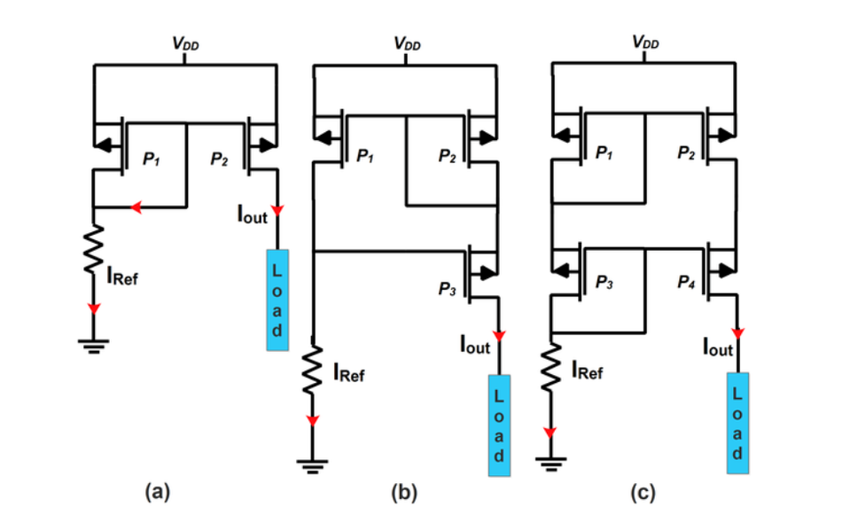
Because current flows relative to the positive rail, the input behaves as a current sink while the output sources current into the load. However, due to hole transport in p-type semiconductor regions, PNP mirrors generally exhibit lower gain and higher distortion than equivalent NPN implementations. Variations in β with collector current can introduce non-linearity, particularly in audio and low-noise amplifier stages. Adding emitter resistors improves current matching and thermal stability, though at the cost of increased compliance voltage. More advanced structures, such as Wilson or cascode mirrors, further enhance output resistance and regulation accuracy.
Applications in Analog Circuits
PNP current mirrors are widely used to provide bias currents and active loads in amplifier stages. For example:
Differential Amplifier Tail Sources – A PNP mirror can serve as the current source feeding the emitter pair of an NPN differential amplifier. This arrangement allows the amplifier to handle signals down to near the negative rail while sourcing current from the positive rail.
Active Loads – Once used at the collector of an NPN transistor, a PNP mirror acts as a high‑impedance load that increases gain and output swing. The mirror’s current is set by a reference resistor or current source.
Current Limiters and Regulators – PNP mirrors can limit the current delivered to a load, provide bias currents in voltage references and serve as building blocks in bandgap reference circuits.
Designers must ensure that the compliance voltage of the mirror is sufficient. The collector of the mirroring transistor must remain reverse-biased by a few hundred millivolts to sustain regulation; otherwise, the mirror enters saturation and the current drops.
Low‑Dropout Regulators and Power Management
PNP Pass Element in LDOs
Low‑dropout linear regulators maintain a constant output voltage even when the input supply is only slightly higher than the output. Linear regulators can use different pass elements: Darlington NPN, single NPN, PNP, PMOS or NMOS transistors. NPN‑Darlington regulators require about 1.6 V of dropout because of two base–emitter drops; NPN regulators reduce dropout to about 0.9 V. Replacing the NPN pass transistor with a PNP reduces the dropout further because the PNP pass device can saturate with very small voltage across it. PNP regulator can achieve dropout voltages as low as 0.15–0.4 V, depending on the device gain. Selecting a high‑gain PNP transistor allows dropout voltages around 150 mV at 100 mA.
The primary trade-off is increased quiescent current. In an NPN regulator, the drive current flows from the input through a PNP transistor and contributes little to the output; the quiescent current is essentially the bias current. In a PNP regulator, the base drive current flows to ground and therefore adds to the output current. The quiescent current can range from 0.8 mA to 2.6 mA. Designs requiring high efficiency at light load often prefer PMOS pass elements. Nonetheless, PNP LDOs remain popular because of their low dropout and simple drive requirements.
Practical Design Considerations
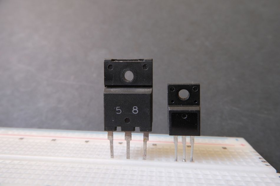
When designing a PNP LDO, choose a transistor with sufficient β at the required current. The error amplifier of the regulator must be capable of sourcing enough base current to drive the pass transistor into saturation when the input voltage approaches the output. Base current flows to ground, so thermal considerations apply. The large PNP power transistor, such as the TIP2955, with a maximum collector current of 15 A and a β of 20–70, can serve as the pass element in a high‑current LDO. Ensure adequate heat sinking to keep junction temperature below 150 °C, and include emitter or collector resistors if necessary to improve stability.
Selecting and Using PNP Transistors
Data‑Sheet Parameters
When selecting a PNP transistor, evaluate the following parameters:
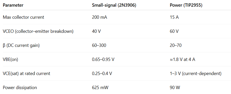
The base–emitter saturation voltage is higher in power devices due to larger junctions. Always consult the data sheet to determine safe operating area (SOA), maximum junction temperature and β vs. collector current characteristics. For high‑frequency designs, check the transition frequency and capacitances. The 2N3906 has a transition frequency around 250 MHz, while the TIP2955 is specified at only a few megahertz.
Thermal and Reliability Considerations
Power PNP transistors dissipate significant power when used as pass elements or high‑side switches. Junction temperature must be kept below the specified limit (150 °C for TIP2955) by using heat sinks and proper PCB layout. Exceeding the safe operating area can cause second breakdown, a failure mode where localized hotspots lead to thermal runaway. Always consult the SOA curves in the data sheet and derate the collector current based on temperature.
Complementary Transistor Pairs
Complementary PNP–NPN pairs, such as TIP2955/TIP3055 or 2N3906/2N3904, are designed to have similar characteristics but opposite polarities. These pairs simplify the design of push–pull amplifiers and power stages. When selecting complementary pairs, match β, transition frequency and saturation voltages to minimize distortion. In integrated circuits, designers often employ lateral PNP transistors because vertical PNPs are difficult to fabricate; these devices generally have lower β but adequate performance for biasing and level shifting.
Selecting and Using PNP Transistors
Choosing between a PNP, NPN, or MOSFET depends on voltage levels, current requirements, efficiency, and control complexity within a solid-state system.
PNP Transistors are best suited for high-side switching, current sourcing, and applications requiring lower voltage headroom, such as low-dropout regulators and bias networks. They are intuitive in bipolar designs but draw base current, which impacts efficiency at light loads.
NPN Transistors are generally preferred for low-side switching, signal amplification, and fast response. They offer higher carrier mobility, better high-frequency performance, and simpler logic interfacing when pulling loads to ground. NPN devices are common in small-signal amplifiers and discrete output stages.
MOSFETs (FETs) excel in power switching and efficiency-critical designs. With voltage-controlled gates and near-zero steady-state gate current, MOSFETs outperform BJTs in high-current and high-speed applications. They are ideal for battery-powered systems, motor drives, and switching regulators, though gate drive and protection requirements are more complex.
In summary, select PNP for high-side bipolar simplicity, NPN for speed and amplification, and MOSFET for efficiency, scalability, and modern power electronics.
Recommended Reading: JFET vs MOSFET: A Comprehensive Engineering Analysis and Selection Guide
Future Trends and Technologies
Although MOSFETs dominate many applications, PNP transistors remain important in analog design, power management and interfacing.
Ongoing research aims to improve PNP performance:
Heterojunction Bipolar Transistors (HBTs) – Using materials such as silicon–germanium, HBTs achieve higher gain and frequency by increasing carrier mobility. PNP HBTs are used in RF amplifiers and high‑speed ICs.
Integrated PNPs in BiCMOS Processes – BiCMOS combines bipolar transistors with CMOS logic. While early BiCMOS processes provided mediocre PNP devices, modern processes offer improved PNP β and frequency, enabling precision analog functions on the same chip as digital logic.
Compound Transistor Configurations – Sziklai pairs and Darlington configurations combine transistors to multiply current gain. In a complementary Darlington pair, an NPN drives a PNP (or vice versa), reducing input drive voltage and delivering high gain.
Power Modules and Integrated Drivers – Many modern power-management ICs integrate PNP pass elements with error amplifiers and protection circuitry, simplifying the design of regulators and high‑side switches.
Understanding the fundamentals described in this article prepares engineers and students to adapt to these innovations.
Conclusion
The PNP transistor is more than a mirror image of its NPN counterpart. By reversing the polarities, designers unlock high‑side switching, complementary amplification and low‑dropout regulation capabilities. This article has explored the physics of PNP devices – their doping, carrier transport and biasing – and shown how these fundamentals translate into practical circuits. We examined switching applications, amplifier stages, current mirrors and regulators, highlighting design procedures and data‑sheet considerations. With this knowledge, engineers can confidently choose between NPN and PNP devices, design bias networks, select appropriate transistors, and exploit complementary pairs for efficient, linear, and robust hardware designs.
Frequently Asked Questions (FAQs)
Q. What is the main difference between NPN and PNP transistors?
A. The key difference lies in the semiconductor doping and current direction. In a PNP transistor, the emitter and collector are p‑type, and the base is n‑type. Majority carriers are holes rather than electrons. Resultantly, current flows from the emitter to the collector and the base must be more negative than the emitter to turn the device on. In an NPN transistor, the polarities are reversed.
Q. How do I bias a PNP transistor for switching?
A. For high‑side switching, connect the emitter to the positive supply and the load between the collector and ground. For high-side switching, connect the emitter to the positive rail and the load to the collector. Drive the base through a resistor sized using Ohm’s law. Pulling the base to a lower voltage forward-biases the device, turning it on.
Q. Can I replace an NPN transistor with a PNP transistor in a circuit?
A. Yes, but all polarities and current directions must be reversed. The emitter connects to the positive rail, bias voltages change, and logic levels must swing sufficiently. In many cases, a FET may be simpler when polarity reversal is impractical.
Q. Why are PNP transistors used in low‑dropout regulators?
A. PNP pass devices allow regulation with very low voltage headroom because they can saturate with minimal collector–emitter drop. This makes them effective solid-state pass elements, although base current increases quiescent current compared to PMOS FET solutions.
Q. What is a complementary Darlington pair, and when is it used?
A. The complementary Darlington (Sziklai) pair combines NPN and PNP devices to achieve high gain with only one base–emitter drop. It is widely used in audio output stages, motor drivers, and switching circuits that require high-current amplification.
Q. What causes the lower frequency performance of PNP transistors compared with NPNs?
A. PNP transistors rely on hole conduction, and holes have lower mobility than electrons. This physical limitation in semiconductor devices increases capacitance and reduces the transition frequency, especially in high-speed output stages and wideband amplifiers.
Q. How do I design a PNP current mirror?
A. Use two matched PNP transistors sharing emitter and base connections. One is diode-connected to set bias; the second mirrors current from the positive rail. Ensure the collector remains at a lower voltage than the emitter to stay in active operation.
References
[1] ScienceDirect. PMOS vs NMOS: Handbook of Analog Circuit Design: Chapter 2 - Basic Amplifier Circuits [Cited 2026 February 10]; Available at: Link
[2] Neexperia. Bipolar Junction Transistor Application Handbook [Cited 2026 February 10]; Available at: Link
[3] Wevolver. PMOS vs NMOS: Unraveling the Differences in Transistor Technology [Cited 2026 February 10]; Available at: Link
[4] Wiki Analog. Chapter 11: The Current Mirror [Cited 2026 February 10]; Available at: Link
in this article
1. Key Takeaways2. Introduction3. Basics of Bipolar Junction Transistors (BJTs)4. Biasing and Operating Regions5. PNP Transistor as a Switch6. Amplifier Circuits using PNP Transistors7. Current Mirrors and Active Loads8. Low‑Dropout Regulators and Power Management9. Selecting and Using PNP Transistors10. Future Trends and Technologies11. Conclusion12. Frequently Asked Questions (FAQs)13. References