Diode Schematic: Theory, Design and Practical Implementation
This in-depth guide explains the physics of PN junction diodes, surveys modern diode types, illustrates a standard diode schematic, explores rectifiers, clippers, and clampers, and offers practical design tips.

16 Dec, 2025. 16 minutes read

Key Takeaways
PN Junction Theory: Diode consists of P‑type and N‑type semiconductor regions joined together. The interface forms a depletion region with a built-in electric field; when forward-biased, the area shrinks and current flows, whereas reverse bias widens the region and blocks current.
Current‑Voltage Relationship: The Shockley equation describes the exponential relation between diode current and voltage. kT/q ≈ 26mV at room temperature. Silicon diodes have forward voltages around 0.7 V, and germanium around 0.3 V.
Variety of Diodes: Beyond the classic rectifier, there are Zener diodes that maintain a constant reverse voltage, Schottky diodes with low forward drop and fast switching, light‑emitting diodes (LEDs) that emit photons when forward biased, and photodiodes that convert light into current and are operated in reverse bias.
Common Circuits: Diodes are used in half‑wave and full‑wave rectifiers to convert AC to DC, clipper circuits to limit signal amplitude, and clamping circuits to shift voltage levels without distorting waveforms.
Introduction
The diode schematic is a fundamental building block in modern electronics, providing engineers with a clear graphical representation of how a diode functions within a circuit. From power rectification to precision voltage regulation, the diode schematic serves as the starting point for analysing device behaviour and predicting circuit performance. It illustrates the orientation, polarity, biasing conditions, and interaction of diodes with surrounding components — critical details for ensuring reliable system performance.
Diode is a two‑terminal semiconductor device that allows current to flow more easily in one direction than the other. The simple symbol of a triangle pointing to a line hints at this unidirectional property, yet the underlying physics and vast array of available devices can seem daunting for newcomers. This article explores the theory behind diode operation, the principles that shape an effective diode schematic, and the practical considerations engineers must evaluate during implementation.
Fundamentals of the PN Junction
Formation of the Depletion Region
The fundamental component of every diode schematic is the PN Junction. This boundary forms where a P-type semiconductor, which has an abundance of holes, meets an N-type semiconductor, which is rich in free electrons. Once the two doped regions are brought together, electrons diffuse from the N-type side into the P-type side, while holes diffuse in the opposite direction. This bidirectional diffusion leads to recombination, leaving behind fixed ionised donor atoms on the N side and ionised acceptor atoms on the P side. These immobile charges create an internal electric field, forming a depletion region devoid of mobile carriers.
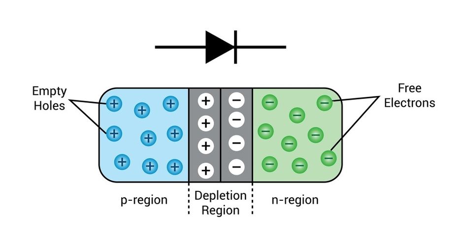
This region acts as an electrostatic barrier that opposes further diffusion, establishing a built-in potential (also called the junction or barrier voltage). For silicon diodes, this potential is typically around 0.7 V, while for germanium it is roughly 0.3 V. [1] The internal electric field always points from the N side toward the P side, driving minority carriers and defining the depletion dynamics.
Once no external bias is applied (zero bias), the depletion region remains stable! Under forward bias, a positive voltage is applied to the P side, partially cancelling the built-in field. The depletion width narrows, allowing carriers to cross the junction easily and enabling a significant forward current. Under reverse bias, the applied field reinforces the built-in potential, widening the depletion region and blocking current except for a small leakage.
The interplay between the built-in voltage, temperature, doping concentration, and external bias determines the I–V characteristics of the diode. This is essential for interpreting a practical diode schematic or diode circuit.
The Shockley Diode Equation
The current that flows through a diode under forward bias is not linear. It follows the Shockley Diode equation:

where:
The equation:
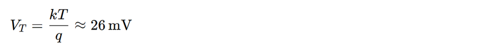
at the room temperature shows:
Forward Bias: Current increases exponentially with voltage
Reverse Bias: The exponential term becomes negligible, and current ≈ −Is
The typical values are:
Silicon Diode: −Is ≈ 10-12 A
Germanium Diode: −Is ≈ 10-6 A
Because the exponential behaviour is steep, engineers often approximate a diode using an ideal diode model with a fixed threshold (≈ 0.7 V Silicon, ≈ 0.3 V Germanium). This simplification is widely used in introductory tutorials, hand analysis, and basic electronic circuits.
Temperature and Doping Effects
Both doping concentration and temperature have strong impacts on diode performance:
Effects of Doping
Heavy Doping → narrower depletion region → lower breakdown voltage and reduced reverse-biased resistance.
Light Doping → wider depletion region → higher breakdown voltage, used in high-voltage rectifier diodes.
Effects of Temperature
Saturation current Is approximately doubles for every 10 °C rise.
Forward voltage decreases by ~2 mV/°C for silicon.
These variations are essential when designing voltage regulators, precision references, or circuits operating in extreme conditions.
Small-Signal Resistance and Junction Capacitance
For AC or small-signal analysis, the diode can be linearised around a bias point.
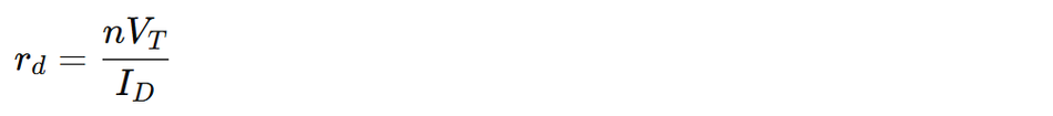
The higher forward current resonates with the lower rd, which influences amplifier gain stages and switching behaviour.
The depletion region behaves like a voltage-dependent capacitor under reverse bias. Increasing reverse voltage widens the depletion region, reducing its capacitance. This property is essential in varactor diodes used in RF tuning circuits and voltage-controlled oscillators.
Recommended Reading: How Does a Diode Work: Unraveling the Heart of Electronic Control
Diode Symbols and Schematic Notation
Diodes are represented in schematics by a triangle pointing towards a vertical bar. The triangle indicates the direction of conventional current flow (from the anode to the cathode), while the bar represents the potential barrier that blocks current in the reverse direction. The figure below illustrates the standard diode symbol.
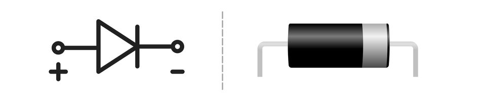
The current flows from the anode (left) through the triangle into the bar, then out of the cathode (right). In physical devices, the cathode end is often marked with a band or stripe.
In some schematics, the triangle is replaced by an arrow pointing toward a vertical line; the concept remains the same. For rectifier diodes, the symbol is simple, but for other diode types, variations exist:
- Zener Diode: The symbol resembles a standard diode, but the cathode bar is replaced with a bent or zigzag line. Indicates controlled reverse breakdown, used in voltage regulators and reference circuits.
- Schottky Diode: Uses a small angled “tick” on the cathode line, showing the metal–semiconductor junction. Recognised for its low forward voltage drop and fast reverse recovery, making it ideal for high-frequency or switching applications.
- Light-Emitting Diode (LED): Standard diode symbol with two arrows pointing away from the junction. Indicates emission of light due to electron–hole recombination.
- Photodiode: Symbol similar to an LED but with arrows pointing toward the junction. It represents light-sensitive operation, widely used in sensors, optical receivers, and solar cells.
Package Orientation and Identification
Manufacturers include polarity markings on packages to reduce assembly errors:
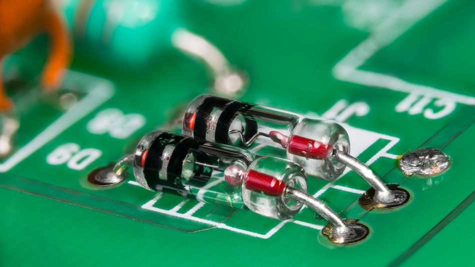
Rectifier Diodes (DO-41, DO-201 Packages): The cathode end has the painted ring; the unmarked end is the anode. [2]
Small Signal Diodes (Glass or Epoxy): Cathode is designated by a band, colour stripe, or printed code.
Light Emitting Diodes (LEDs):
Long Lead = Anode
Short Lead = Cathode
The cathode side often has a flat edge or a notch on the plastic lens.
SMD Diodes (SMA, SMB, SMC): The bar printed on the package marks the cathode; device datasheets describe additional polarity indicators.
Once interpreting a diode schematic, correct orientation is essential! The reversed diode may block current, distort signals, cause incorrect biasing, or lead to component damage, especially in high-voltage or reverse-biased applications.
Recommended Reading: Diode, Anode, Cathode: Unlocking the Power of Semiconductor Junctions
Survey of Diode Types
Standard Rectifier Diode
The standard PN rectifier diode is the backbone of many electronic circuits, especially in power conversion! Built to handle relatively high forward currents and substantial reverse voltage stress, it is commonly used in bridge rectifiers, power supplies, and DC conversion systems. Its I–V characteristic follows the Shockley equation: under forward bias, a silicon rectifier exhibits a 0.6–0.8 V drop, while under reverse bias, only a minute leakage current flows until the breakdown voltage is reached. [3]
In practical rectifier diodes, designers look at several parameters:
Maximum Forward Current: The highest continuous current the device can conduct without exceeding its thermal limits. Small-signal diodes handle milliamps; power rectifiers may handle tens or hundreds of amperes.
Peak Inverse Voltage (PIV): The maximum reverse voltage the diode can withstand safely. Good practice is to choose a PIV rating at least 1.5–2× the peak AC voltage in rectifier designs.
Reverse Recovery Time: The interval required for a diode to switch from conduction to blocking. The standard power rectifiers may have the reverse recovery time in tens of microseconds, whereas fast recovery diodes achieve nanosecond speeds.
Package and Thermal Resistance: Current handling and junction temperature are strongly influenced by packaging (DO-41, TO-220, TO-247) and required heatsinking.
Rectifier diodes represent the “typical diode” form factor encountered in power electronics.
Zener Diode
The Zener diode is a specially doped PN junction designed to operate in the reverse breakdown region without damage.

Once reverse voltage exceeds a characteristic Zener voltage, the diode conducts strongly while maintaining a nearly constant voltage across it. Forward biased, it behaves like a normal diode (0.7 V drop). Zener diodes are used as voltage references and regulators because their voltage remains stable over a wide range of current.
The key characteristics include:
Reverse Biased Operation: The cathode is connected to the positive supply, enabling load regulation when combined with a series resistor that limits current and prevents excessive power dissipation.
Zener Voltage Range: The common values span from 2.4 V to several hundred volts. Low-voltage Zeners (<5 V) exhibit tunneling breakdown, while higher-voltage types use avalanche breakdown.
Temperature Coefficient: Low-voltage Zeners have a negative coefficient; high-voltage Zeners have a positive one. Precision references often combine Zeners to approximate zero drift.
Because Zener diodes hold voltage nearly constant under varying load conditions, they are widely used in reference generators, overvoltage protection, and simple shunt regulators.
Schottky Diode
The Schottky diode uses a metal–semiconductor junction instead of a PN junction.
Because it involves only majority carriers (no minority‑carrier recombination), it has a much lower forward voltage drop, typically 0.3–0.5 V, and extremely fast switching times (nanoseconds). This makes Schottky diodes ideal for high‑frequency rectification, power supply free‑wheeling diodes and logic level shifting. The trade‑off is higher reverse leakage current and lower breakdown voltage than standard PN diodes.
In digital design, Schottky diodes are used in transistor‑transistor logic (TTL) families (e.g., 74LS) to prevent transistor saturation, thus reducing propagation delay. In power electronics, they appear as “flyback” diodes across inductive loads to catch voltage spikes.
Light‑emitting diode (LED)
When a PN junction is heavily forward-biased, electrons and holes recombine and release energy. In light‑emitting diodes, the semiconductor material is chosen so that recombination emits photons instead of phonons; the bandgap determines the colour. The forward voltage drop depends on the material and typically ranges from 1.2 V (infrared) to 3.6 V (blue or white). Typical forward currents are 10–30 mA.
Because LEDs have no inherent current limiting, a series resistor must be used to set the current. The resistor value is calculated as:
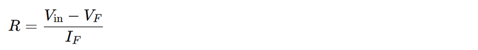
where V(in) is the supply voltage, V(F) is the LED forward voltage, and I(F) is the desired forward current. Failure to include a resistor can destroy the diode due to runaway current.
LEDs are used for indicators, displays, optical communications and lighting. Modern high‑brightness LEDs incorporate multiple junctions and phosphor coatings to produce broad‑spectrum white light.
Photodiode
Photodiode is a PN or PIN junction designed to convert light into an electrical current. When photons strike the depletion region, they generate electron–hole pairs, which are swept by the internal field, producing a photocurrent. In darkness, the junction has high resistance; as light increases, the resistance drops and the current increases.
Photodiodes are usually operated in reverse bias to widen the depletion region, reduce junction capacitance and improve linearity. The photocurrent is roughly proportional to the incident light power.
There are several photodiode varieties:
PIN Photodiode: Includes an intrinsic layer between P and N regions, increasing the depletion width and improving sensitivity.
Avalanche Photodiode: Operated near breakdown; multiplication increases sensitivity but also noise.
Schottky Photodiode: Uses a metal–semiconductor junction for very fast response but lower sensitivity.
Photodiodes are useful in optical communications, camera sensors, smoke detectors and other light‑sensing applications. When reading a photodiode schematic, remember that current flows in the opposite direction of a normal diode — light‑generated current flows from cathode to anode.
Tunnel, Varactor, and Other Special Diodes
While rectifiers, Zeners, Schottkys, LEDs and photodiodes cover most practical needs, a handful of specialised diodes are worth mentioning:
Tunnel Diode: Extremely heavily doped PN junction exhibiting negative differential resistance due to quantum tunnelling. Historically used in microwave oscillators and amplifiers.
Varactor (Varicap) Diode: Exploited for its voltage‑dependent capacitance in tuned circuits. Under reverse bias, the junction capacitance varies with applied voltage, enabling voltage‑controlled oscillators (VCOs).
Step Recovery Diode: Engineered to store charge and abruptly release it, generating harmonics for frequency multipliers.
Avalanche Diode: Similar to Zener but optimised for high breakdown voltages and used to protect circuits from surges.
Comparison of Diode Types
The following table compares the most common diode types. The forward voltage drop is typical; actual values depend on current and device construction.
| Diode Type | Forward Voltage Drop | Breakdown/ Special Voltage | Key Features | Typical Applications |
| Rectifier (Silicon) | 0.6 – 0.8 V | 50 V – 1000 V | Robust, Handles High Current | Power Rectification |
| Rectifier (Germanium) | 0.2 – 0.3 V | 10 V – 50 V | Low Threshold, High Leakage | RF Detection, Mixer Circuits |
| Zener | 0.6 – 0.8 V (Forward) | 2.4 – 200 V (Reverse) | Constant Reverse Voltage | Voltage Reference, Regulator |
| Schottky | 0.2 – 0.5 V | 20 V – 200 V | Low Forward Drop, Fast Switching | Switching Supplies, Logic Clamping |
| LED | 1.2 – 3.6 V | N/A | Emits Light; Color Dependent on Bandgap | Indicators, Displays, Illumination |
| Photodiode | ~0.3 – 0.7 V (Photovoltaic Mode) | 10 – 100 V (Reverse Bias) | Generates Current when Illuminated | Photodetectors, Solar Cells |
| Varactor | N/A (Reverse Biased) | Voltage‑Dependent Capacitance | Tunable Capacitance | Radio Tuners, VCOs |
| Tunnel | ~0.1 V | Negative Resistance Region | Very Fast, Limited to Specific Niches | Microwave Oscillators |
Recommended Reading: Understanding Silicon Controlled Rectifiers: Theory, Design and Practical Implementations
Fundamental Diode Circuits
Half-Wave Rectifier
A half-wave rectifier uses a single diode to convert an alternating current (AC) waveform into a pulsating direct current (DC). During the positive half cycle of the AC input, the diode becomes forward-biased, allowing current to flow through the load. During the negative half cycle, the diode is reverse-biased, blocking current and producing zero output. The result is a unipolar, highly rippled DC waveform at the input frequency.
For a sinusoidal input, the average output voltage is:
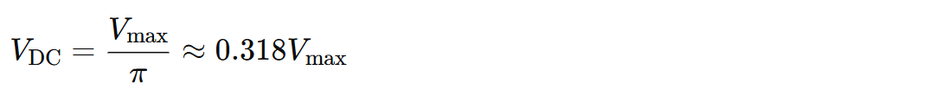
This low conversion efficiency (≈40%) and high ripple make half-wave rectifiers suitable mainly for low-power or low-cost applications such as signal demodulation, basic power supplies, and educational circuits. A transformer is often used to adjust the supply voltage before rectification.
Full‑Wave Rectifier
A full-wave rectifier uses both halves of the AC waveform, doubling the ripple frequency and producing a smoother DC output.
The two common implementations exist:
1. Centre‑Tapped Full‑Wave Rectifier: This configuration uses a transformer with a centre-tapped secondary and two diodes.
On the positive half cycle, one diode conducts
On the negative half cycle, the other diode conducts
The output is the absolute value of the input, with an average DC voltage ≈ 0.637 V (max)
Limitations include the need for a centre-tapped transformer and the requirement that each half of the winding must withstand the full peak voltage.
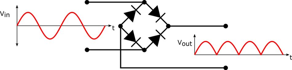
2. Bridge Rectifier: The four-diode bridge rectifier eliminates the need for a centre-tapped transformer. During each half cycle, two diodes conduct, resulting in a forward drop of roughly:
~1.4 V for silicon diodes
~0.5–0.7 V if Schottky diodes are used
Because the ripple frequency is doubled, filtering becomes easier, and the output is smoother.
Smoothing capacitors are usually added to reduce ripple. When the load current is small relative to the capacitor’s discharge rate, the output approaches a steady DC value. For heavy loads, multi‑stage filters or regulators are used.
Clip and Clamp Circuits
Clipper Circuits
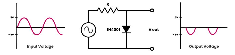
Clipper circuits remove portions of an input waveform that exceed a set amplitude. They protect sensitive circuits from overvoltage and shape signals. A simple negative clipper places a diode in parallel with the load in reverse orientation so that when the input goes negative, the diode conducts and clamps the output near −0.7 V. A positive clipper is similar but oriented to clip positive peaks. Symmetrical clippers use two anti‑parallel diodes to clip both positive and negative peaks at ±0.7 V. Adding series resistors or combining diodes with DC sources allows customised clipping levels.
Clipper circuits are often used on audio and instrumentation inputs to prevent saturating amplifiers. Zener diodes can provide precise clipping at arbitrary voltages; for instance, placing a 5.1 V Zener across a logic input clamps the voltage to within safe CMOS limits.
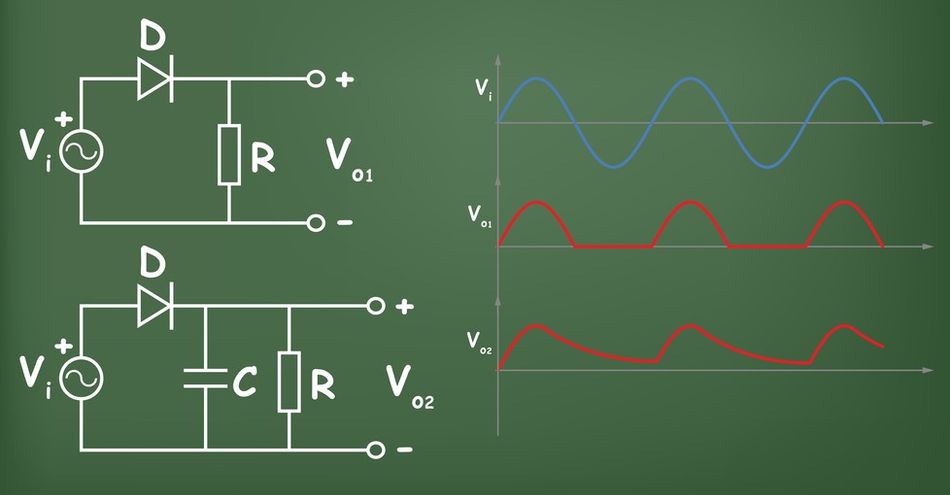
Clamper Circuits
A clamp circuit shifts the entire waveform up or down without altering its shape, effectively adding a DC offset. The typical positive clamper consists of a diode, a capacitor, and a resistor. During the negative half-cycle, the diode conducts and charges the capacitor to its peak amplitude. On the positive half cycle, the capacitor adds its stored voltage to the input, shifting the waveform upward.
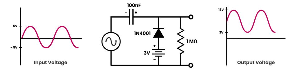
Unlike a clipper, a clamper does not remove peaks; it slides the waveform along the voltage axis. Positive clampers raise the minimum of the waveform to a desired level; negative clampers lower the maximum. Proper choice of the RC time constant ensures the capacitor holds its charge over many cycles. The clampers are used in oscilloscope coupling, signal restoration and DC restoration in communication receivers.
Diode Logic and OR Gating
In digital design, diodes can implement simple logic functions. Diode OR gating connects multiple diode cathodes with their anodes tied to input signals. The output is pulled high through a resistor; any input that goes high (logic 1) forward-biases its diode, forcing the output high. This forms a wired‑OR function. Similarly, diode AND gating is achieved by using diodes in reverse orientation on negative logic levels.
While the diode logic cannot provide amplification or buffering, it is still used in interrupt line combining, level shifting, and simple control logic in power supplies and embedded systems.
Practical Design Considerations
Selecting a Diode
Choosing the appropriate diode for a diode circuit requires evaluating multiple electrical, thermal, and mechanical factors.
The key parameters include:
Forward Current Rating: Ensure I (F, max) exceeds the expected load. For power supplies, add a safety margin (≥20 %). Consider surge current ratings for rectifiers handling inrush currents from capacitor charging.
Reverse Voltage Rating: Choose a PIV at least twice the peak input voltage to account for transients. High-voltage circuits often require derating per temperature or humidity specifications.
Switching Speed: Fast diodes are required for high‑frequency rectifiers, RF detectors and digital logic. Schottky or fast‑recovery diodes may be appropriate. Standard rectifiers are unsuitable when the reverse recovery time affects circuit timing or efficiency.
Thermal Management: Check power dissipation and provide heat sinking if needed. Many diodes are rated at 25 °C ambient; derate the current at higher temperatures. Use proper heat sinking or choose packages with low thermal resistance (TO-220, TO-247) for high-current paths.
Package and Footprint: Ensure the package fits mechanical constraints and assembly process (through‑hole vs surface mount). For high‑current diodes, low-thermal-resistance packages (e.g., TO‑220) are preferred.
Reading Diode Datasheets
Manufacturers provide datasheets with graphs and tables showing I–V curves, capacitance vs reverse voltage, reverse recovery time and thermal characteristics. When interpreting a diode schematic, refer to the datasheet to understand how the device behaves under operating conditions. Pay particular attention to curves of forward current vs forward voltage at different temperatures and to maximum ratings.
Using Diodes in Combination
Many diode circuits use diodes in series or parallel to achieve desired voltages or currents. For example, connecting diodes in series increases the total forward drop; connecting them in parallel shares current (although balancing resistors are required). In high‑voltage rectifiers, multiple diodes may be stacked in series with balancing resistors to share reverse voltage. In LED strings, a resistor or constant‑current driver ensures each diode receives the same current.
Safety and Surge Protection
Diodes are used to protect circuits from voltage spikes. Flyback diodes across inductive loads (relays, motors) provide a path for stored energy when the supply is switched off, preventing damaging voltage spikes. Transient voltage suppressor (TVS) diodes are specialised avalanche diodes designed to clamp high‑energy transients (e.g., lightning, electrostatic discharge). They respond much faster than ordinary Zeners and are specified by standoff voltage and peak pulse current.
Market Trends and Future Directions
Diodes remain foundational components in modern electronics, from smartphone chargers and IoT sensors to automotive powertrains and high-power industrial inverters.
In 2025, the global diode market reached USD 18.16 billion and is forecasted to grow to USD 24.58 billion by 2030, representing a 6.24% CAGR. [4] The Asia–Pacific region dominates with approximately 58.86% of global revenue, driven by rapid expansion in consumer electronics manufacturing, electric vehicle production, and industrial automation. Within the overall market, laser diodes hold the largest segment, about 36.1%, and are projected to grow at 8.6% CAGR, owing to rising demand in optical communication, sensing, and advanced display technologies.
Several technological shifts are expected to influence future diode schematics, design methodologies, and system-level architectures:
Wide-Bandgap Semiconductors
Emerging materials such as silicon carbide (SiC) and gallium nitride (GaN) offer superior characteristics: higher breakdown voltage, lower reverse recovery, and dramatically improved efficiency.
SiC Schottky Diodes already replace traditional silicon rectifiers in high-frequency SMPS, EV charging systems, and photovoltaic inverters.
GaN-based Diodes and transistors support ultra-fast switching, enabling smaller magnetics and greater power density.
Integrated Photonics
The convergence of photodiodes, LEDs, and electronic control circuits on a single silicon substrate is transforming high-speed communication and sensing.
CMOS Image Sensors rely on vast photodiode arrays with low noise and high quantum efficiency.
LiDAR Modules, AR/VR depth sensors, and autonomous-vehicle perception systems depend heavily on integrated laser diodes and photodiodes for precise time-of-flight measurement. This integration reduces latency, improves bandwidth, and lowers overall energy consumption.
Miniaturisation and Advanced Packaging
The electronic systems are shrinking each passing day, so the diode packaging continues to evolve:
Ultra-compact SOD-123, SOD-323, and chip-scale packages reduce parasitic inductance and improve high-frequency performance.
Flip-chip LEDs and thermally enhanced packages deliver better heat spreading and higher lumen output in lighting applications.
The compact packaging also enhances electromagnetic compatibility, a key requirement for 5G devices and automotive electronics.
Smart Lighting and Energy-Efficient Illumination
High-power LEDs with integrated drivers are rapidly replacing incandescent, halogen, and even fluorescent lighting technologies.
Improvements in phosphor coatings, quantum-dot materials, and thermal interfaces increase luminous efficiency and colour rendering.
The digital lighting systems, such as tunable white LEDs and Li-Fi communication modules, rely on advanced diode structures for reliability and modulation speed.
Understanding diode schematics in the context of these trends helps engineers design next‑generation devices and systems.
Recommended Reading: What Are Schematics: The Blueprint Language of Engineering Decoded
Conclusion
Diodes remain among the most essential electronic components, enabling functions ranging from simple rectification to precision sensing, optical communication, and high-efficiency power conversion. The diode schematic represents a PN junction that allows current to flow primarily in one direction. The Shockley equation describes the exponential I–V relationship, while simple threshold approximations aid circuit design. Engineers choose from rectifiers, Zener, Schottky, LED, photodiode, tunnel and other specialised diodes, each with unique behaviours and schematic symbols. Mastery of diode fundamentals enables the design of rectifiers, clippers, clampers, voltage references, photodetectors and digital gating circuits. Innovations in materials (GaN, SiC), packaging, and integration will push diode performance to new levels. These innovations not only expand diode performance but also reshape how circuits are designed, protected, and optimised.
Frequently Asked Questions (FAQ)
Q. What is the difference between a diode and a Zener diode?
A. The standard diode conducts in the forward direction and blocks reverse current from a voltage source. In contrast, a Zener diode is engineered to regulate diode voltage under controlled reverse breakdown, providing stable bias voltage in real-world circuits.
Q. How can I determine the orientation of a diode on a schematic or PCB?
A. In schematics, current flows from the positive side to the negative side of the symbol. On PCBs, the cathode is band-marked; verify polarity using a multimeter in diode-test mode for real-world accuracy.
Q. How does a Schottky diode achieve a lower forward voltage drop?
A. Schottky diodes use a metal–semiconductor junction rather than a PN junction. Since only majority carriers participate, there is no minority‑carrier storage, and the forward voltage is lower, around 0.3–0.5 V. This also results in fast switching times.
Q. What determines the ripple in a rectifier circuit?
A. Ripple depends on waveform usage, capacitor size, and load current. Applying Ohm’s law to the discharge path helps estimate ripple behaviour, especially when using reverse-biased diodes in smoothing networks for real-world power supplies.
Q. Can I connect diodes in parallel to increase current handling?
A. It is possible, but because diodes have slightly different forward voltages, one diode may carry more current than the other. To balance currents, include ballast resistors in series with each diode. Manufacturers sometimes provide matched diode arrays for this purpose.
Q. How does temperature affect diode behaviour?
A. Once the temperature rises, the reverse saturation current increases and the forward voltage decreases (roughly −2 mV/°C for silicon). High temperatures may also reduce breakdown voltage. It is better to check the datasheet for temperature coefficients and derate the current accordingly.
References
[1] Wevolver. Forward Bias, Reverse Bias and their effects on Diodes [Cited 2025 December 10] Available at: Link
[2] Toshiba. How to Distinguish the Anode and Cathode Terminals of a Diode? [Cited 2025 December 10] Available at: Link
[3] MSAJCE. PN Junction Diode: Structure, Operation & V-I Characteristics [Cited 2025 December 10] Available at: Link
[4] Mordor Intelligence. Diode Market Size & Share Analysis - Growth Trends And Forecast (2025 - 2030) [Cited 2025 December 10] Available at: Link
in this article
1. Key Takeaways2. Introduction3. Fundamentals of the PN Junction4. Diode Symbols and Schematic Notation5. Survey of Diode Types6. Comparison of Diode Types7. Fundamental Diode Circuits8. Practical Design Considerations9. Market Trends and Future Directions10. Conclusion11. Frequently Asked Questions (FAQ)12. References