H Bridge Motor Driver: Complete Engineering Guide to Topologies, ICs, and PCB Layout (2026)
This guide offers engineers an in-depth understanding of H Bridge motor driver, explaining its basics, circuit topologies, device selection, driver IC comparisons, printed circuit design and practical considerations for next generation projects.

Last updated on 22 May, 2026. 17 minutes read
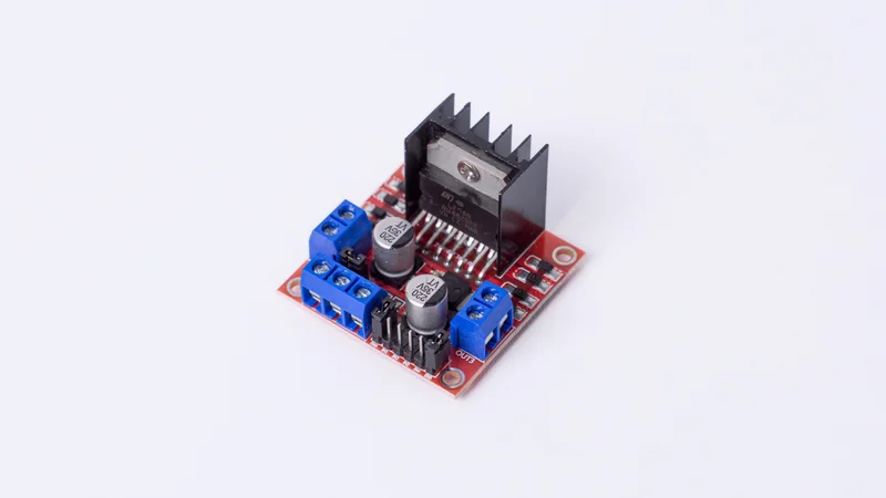
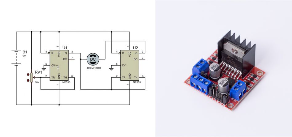
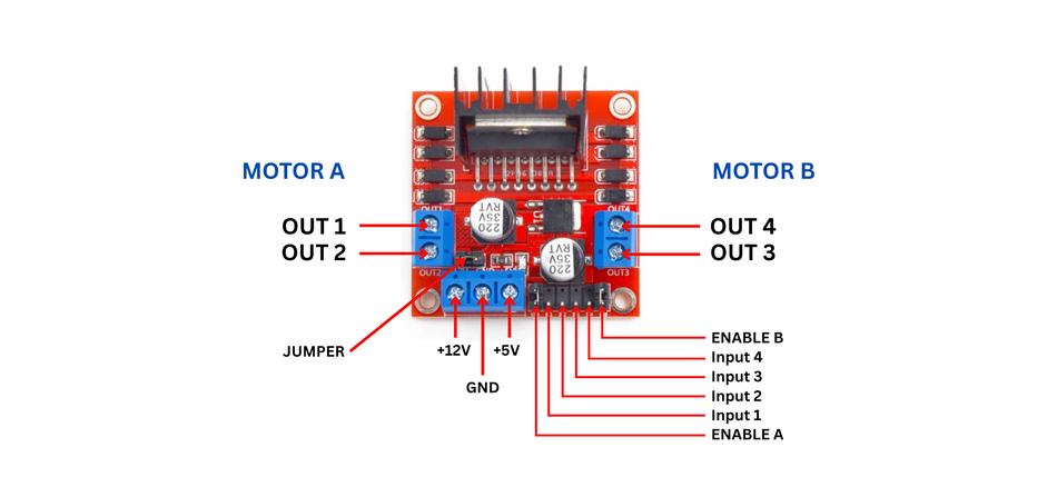
Dual, H-Bridge DC Motor Controller Board
Key Takeaways
H Bridge Motor Driver uses four switches to reverse the polarity applied to a load, enabling bidirectional speed control for brushed DC motors and stepper motors.
Modern Drivers rely on MOSFETs or wide‑bandgap devices for low on‑resistance and fast switching; proper dead time prevents shoot‑through when switches commutate.
Gate Driver ICs integrate charge pumps, current regulation, diagnostic flags and programmable slew rates; selecting the right driver involves balancing voltage range, current rating and protection features.
PCB Layout is critical: minimize high‑current loop areas, place decoupling capacitors close to devices and use wide copper and thermal vias to manage heat and reduce inductance.
Shoot‑through arises from parasitic capacitances (Miller effect); mitigation techniques include gate resistors, active Miller clamps and appropriate dead‑time settings.
Step‑by‑Step Methodology — from load specification to simulation — helps engineers choose devices, design gate drivers, size components, and validate thermal performance.
Introduction
The electric‑motor applications span robots, automotive actuators and industrial drives. These systems need precise control over direction and torque while minimising losses. The H bridge motor driver topology uses power switches to steer current through the motor in either direction. Over the past decade, advances in MOSFET technology, wide‑bandgap semiconductors and integrated driver ICs have transformed H‑bridge performance.
Modern drivers support higher voltages and currents, integrate gate‑drive functionality and offer sophisticated protections such as overcurrent shutdown, shoot‑through prevention and thermal monitoring. This guide offers an in-depth understanding of the H Bridge motor driver, explaining its basics, circuit topologies, device selection, driver IC comparisons, PCB layout best practices and practical considerations for next-generation projects.
Basics and Evolution of H‑Bridge Motor Drivers
History and Fundamentals
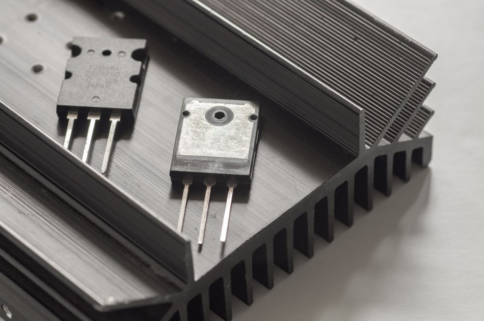
The H bridge derives its name from the arrangement of four switches that resemble the letter "H." Early implementations used electromechanical relays, with double‑pole double‑throw (DPDT) relays providing bidirectional current flow. Relay‑based H bridges suffer from slow switching, audible noise and wear. Semiconductor progress replaced mechanical contacts with transistors, enabling faster switching and finer control. Today, designers typically employ MOSFETs for their high input impedance and low on‑resistance, though IGBTs or BJTs may be used in high‑voltage or high‑current applications.
The basic H bridge comprises four switches: two high‑side devices connecting to the positive supply and two low‑side devices connecting to ground. By controlling the on/off states of these switches, the voltage applied across the motor can be reversed or turned off. For example, turning on the upper left and lower right transistors drives current forward; turning on the upper right and lower left reverses direction. Turning on both low‑side switches allows current to recirculate during pulse‑width modulation (PWM), enabling efficient control of torque.
Relay‑Based H Bridges
In low‑speed applications such as hobby robots or 12 V automotive actuators, relays can still provide a simple H‑bridge implementation. DPDT relay toggles polarity while a separate transistor controls current magnitude.
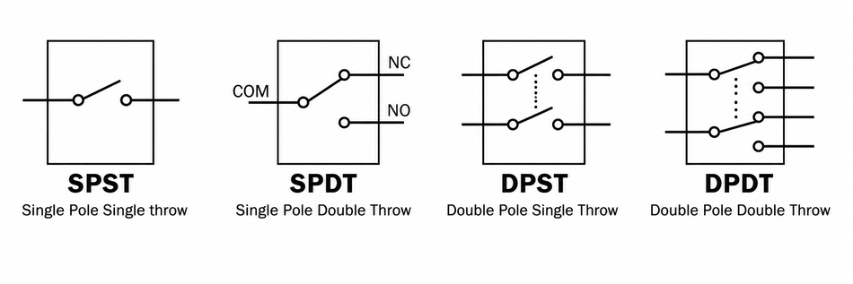
Combining relay direction control with a MOSFET for PWM reduces wear on relay contacts. However, relay switching times in the millisecond range limit PWM frequency and introduce audible clicking, making solid‑state solutions preferable for precision control.
Semiconductor‑Based H Bridges
Modern H bridges generally adopt one of three transistor configurations:
Complementary Design (P‑channel High Side, N‑channel Low Side) – The high‑side devices are P‑channel MOSFETs or PNP BJTs, simplifying gate drive because the gate reference is ground. The low‑side uses N‑channel devices. This arrangement suits low‑voltage circuits but suffers from higher on‑resistance due to the P‑channel devices.
N‑channel MOSFET Design – Four N‑channel MOSFETs provide the lowest conduction losses. Because N‑channel devices require gate voltage above the supply rail to turn on in the high‑side position, designers use charge‑pump‑based gate drivers, isolated DC‑DC converters or gate‑drive transformers. This topology is standard in high‑efficiency motor controllers and synchronous buck converters.
Half‑Bridge and Derived Topologies – The half‑bridge uses two switches and cannot reverse motor polarity but is common for unidirectional drives, synchronous rectifiers and audio power amplifiers. A three‑phase inverter extends the H bridge by adding additional legs for polyphase motors. Half‑controlled rectifiers replace one switch with a diode to prevent reverse current.
Wide‑Bandgap and Emerging Devices
Gallium Nitride (GaN) and SiC MOSFETs offer lower switching losses and faster transients compared with silicon. Designers considering these devices must pay attention to gate‑charge characteristics and Miller capacitance.
Parasitic gate‑drain capacitance in wide‑bandgap devices can inject currents into the complementary switch during high dv/dt transitions, potentially causing shoot‑through. Mitigation strategies such as active Miller clamps, negative gate‑bias voltage and careful gate‑driver selection become even more important.
Recommended Reading: SiC MOSFET: Wide-bandgap Power Devices for High-Efficiency Converters
Understanding the H Bridge Topology
Basic Operation and Switching States
H bridge is a core motor control topology widely used for driving direct current motors in robotics, automation, and industrial systems. It consists of four switching elements — most commonly MOSFETs or, in some cases, IGBTs — arranged so that the load is connected between the midpoints of two half-bridges. The top switches (S1 and S2) connect to the positive power supply, while the bottom switches (S3 and S4) connect to ground (GND).
Activating one diagonal pair (S1 and S4) creates current flow through the motor in the forward direction. Activating the opposite diagonal (S2 and S3) reverses the polarity, enabling bidirectional operation. Turning on both high-side switches or both low-side switches shorts the motor terminals, creating a dynamic brake that dissipates kinetic energy through intrinsic diodes. Turning all switches off lets the motor coast as inductive energy circulates naturally.
Digital control platforms achieve variable speed by using Pulse Width Modulation (PWM). The controller modulates the duty cycle of the driving signals, effectively adjusting the average voltage across the motor. Because DC motors act as first-order systems with electrical and mechanical time constants, the average current and torque respond smoothly to PWM even though the voltage waveform is pulsed.
Avoiding Shoot-Through and the Need for Dead Time
One of the critical design requirements is preventing shoot-through: a short circuit from the supply to ground when both the high-side and low-side devices in one leg conduct simultaneously. Shoot-through can destroy transistors and cause substantial current spikes.
Engineers introduce a small dead time, typically 100–300 ns for silicon MOSFETs, to allow one device to turn off completely before turning on its complement. Many integrated gate driver chips provide configurable dead time and interlock logic to eliminate overlaps.
The H Bridge as a Polarity Reverser
Mathematically, an H bridge acts as a bidirectional chopper. The motor current Im(t) obeys the differential equation:

Here, Vdc is the supply voltage, Eb is the back electromotive force proportional to motor speed, Rm and Lm are the motor’s resistance and inductance, and σ represents the switching state (+1 forward, -1 reverse, 0 coast). The mechanical torque tau is proportional to current as:

By changing sigma through PWM, both direction and torque magnitude can be controlled. The symmetry in ±σ ensures identical performance in forward and reverse if the electronic circuit is balanced.
Device Selection: MOSFETs, IGBTs and Wide‑Bandgap Devices
Selecting the appropriate switch technology depends on voltage, current, switching frequency and cost. MOSFETs dominate low‑voltage (5 V–200 V) applications because of their low gate drive power and fast switching. The key parameters include drain‑source breakdown voltage, continuous drain current, drain-source on-resistance and thermal resistance.
IGBTs combine a MOSFET gate with a bipolar output structure, providing high voltage ratings (>600 V) and robust conduction at the expense of slower switching and a conduction knee voltage. IGBTs are common in motor drives over 100 W and in inverters. Wide‑bandgap devices (GaN or SiC) offer even higher voltage and temperature capabilities with extremely low switching losses, enabling switching frequencies above 100 kHz and high power density.
Designers must also select body‑diode characteristics and consider reverse‑recovery current; slow diodes can increase switching losses and cause shoot‑through. For high‑side MOSFETs, choose devices with low gate‑drain (Miller) capacitance to reduce susceptibility to dv/dt‑induced turn‑on. Once using wide‑bandgap devices, ensure the gate driver can provide the required negative gate bias and rapid turn‑off to avoid cross‑conduction.
Recommended Reading: Why IGBTs Remain Relevant in the Era of SiC and GaN Power Devices?
Design Methodology: 7 Steps to an H‑Bridge Motor Driver
Designing an H-bridge circuit for DC motor control requires balancing electrical performance, cost, reliability, and ease of integration. The following steps summarise a proven workflow for designing an H bridge motor driver:
1. Specify Electrical Requirements
Identify the nominal voltage, continuous current, peak current and desired speed or torque range of the motor. Here, you need to consider environmental extremes, supply fluctuations, and fault conditions.
For example, a 24 V DC motor with 10 A continuous and 20 A peak current should use components rated for at least 40 V and 30 A to accommodate transients and prevent short circuit failures.
2. Select Switches and Topology
Select between MOSFETs and IGBTs based on the required voltage and current. For MOSFETs, ensure the drain-source voltage rating is at least 1.3 times the nominal voltage, and select devices with low on-resistance to minimize conduction loss:

Wide-bandgap devices like GaN and SiC offer lower losses and faster switching, though at a higher cost. Decide whether to use discrete transistors or integrated H-bridge motor drivers. Integrated ICs often include protection, diagnostics, and built-in driver circuits.
3. Choose Gate Drivers
A proper driver IC can make or break the design. It must provide sufficient gate charge at the target PWM frequency to turn on the MOSFETs fully, and it should include dead time control to prevent shoot-through. High-side drive often requires bootstrap capacitors or charge pumps to handle polarity changes across motor terminals. Evaluate the common-mode transient immunity and propagation delay of the driver to ensure robust operation at desired switching speeds.
4. Set PWM Frequency and Dead Time
Select a Pulse Width Modulation (PWM) frequency that balances audible noise and switching losses. Frequencies between 20 kHz and 100 kHz are common; 25 kHz is above the upper threshold of human hearing. Dead time should exceed the maximum turn-off time of the MOSFET plus margin.
For example, if the MOSFET turns off in 50 ns, a dead time of 200 ns provides safety. Too much dead time reduces effective voltage and increases ripple.
5. Incorporate Current Sensing and Protection
Use shunt resistors, Hall-effect sensors, or current transformers for real-time monitoring. Overcurrent protection safeguards against high current faults, while undervoltage and thermal protection prevent damage from extreme conditions. The majority of H-bridge motor drivers integrate torque detection and current flow monitoring for enhanced safety.
6. Provide Freewheel Paths
Motor inductance resists abrupt current changes, causing voltage spikes when switches turn off. Use the body diodes or external fast diodes in MOSFETs to allow current to flow during off periods. The choice affects reverse recovery losses and efficiency.
7. Simulate and Prototype
Before committing to hardware, simulate the circuit using tools such as LTspice 24 or QSPICE to analyze transients, switching losses, and schematic optimization. Transient analysis further reveals voltage overshoot, current ripple and required dead time. Frequency response analysis in LTspice 24 allows control loop design. QSPICE supports large digital logic blocks and can generate MOSFET models from datasheet data.
Once the simulation is completed, now build a prototype on a development board and verify performance with oscilloscopes and current probes.
Recommended Reading: How Do MOSFETs Work: Comprehensive Technical Guide for Engineers
Driver IC Comparison: L298, DRV8871, BTN7960 and NovalithIC
Let’s compare the popular H bridge motor driver options below:
L298: Bipolar Technology for Low‑Voltage Dual Motor Drivers
The ST L298 is a monolithic dual full‑bridge driver fabricated in bipolar technology. It operates up to 46 V and provides 2 A DC per channel, with a peak non‑repetitive current of 3 A. The device requires external power transistors and freewheel diodes. [1] It offers separate logic and motor supply pins, TTL‑compatible inputs and over‑temperature protection. With minimal integrated protection, the L298 is best suited for small robots and stepper motors where discrete MOSFETs are unnecessary.
DRV8871: Integrated MOSFET Driver with Current Regulation
DRV8871 integrates two N‑channel MOSFETs with a typical drain-source on-resistance of 565 mΩ and supports motor voltages from 6.5 V to 45 V. The driver can handle 3.6 A peak current and features built‑in current regulation using an internal sense amplifier, eliminating external sense resistors. [2] It includes undervoltage lockout, overcurrent protection, thermal shutdown and a low‑power sleep mode. The small 8‑pin package makes it ideal for portable devices requiring efficient control without heat sinks.
BTN7960: High‑Current Module with Slew‑Rate Control
The BTN7960 module comprises two BTS7960 NovalithIC half‑bridge ICs configured as an H bridge. Each half‑bridge integrates a p‑channel high‑side MOSFET, an n‑channel low‑side MOSFET and a driver. The module accepts 6–27 V input, delivers up to 43 A peak current and supports PWM frequencies up to 25 kHz. [3] Slew rate and dead time are adjustable; current sense and fault status outputs provide diagnostics. Its integrated protections make it suitable for hobby electric vehicles and robot arms.
NovalithIC BTN7930/BTN7970: Automotive‑Grade Half‑Bridges
NovalithIC half-bridges incorporate a p‑channel high‑side MOSFET, an n‑channel low‑side MOSFET, a driver with integrated charge pump and protection circuits. The BTN7930 offers a typical path resistance of 55 m+-Ω, supports PWM up to 25 kHz with active freewheeling and provides current limitation from 20 A to 32 A. Built‑in diagnostics include a status flag and current‑sense feedback. Over‑temperature and over/under‑voltage protections ensure automotive reliability. Designers choose NovalithIC devices when they need high current, adjustable slew rate, dead time generation and simplified heat‑sinking in a compact package.
PWM Frequency, Dead Time and Shoot‑Through Prevention
Choosing PWM Frequency
The PWM frequency affects motor response, audible noise and switching losses. Frequencies around 20 kHz eliminate audible whine for most motors while keeping switching losses manageable. Some low‑voltage motors tolerate higher frequencies (>50 kHz), but designers must check MOSFET and driver datasheets for maximum switching speed and gate‑charge requirements. When using current‑control schemes, choose a frequency high enough to sample current accurately; a typical range is 10–50 kHz.
Dead‑Time Insertion
Dead time is the interval between turning off one transistor and turning on the other in a half‑bridge. Too little dead time risks shoot‑through; too much increases current ripple and reduces effective duty cycle. The required dead time depends on MOSFET transition times, gate resistor values and supply voltage. Gate‑driver ICs often provide programmable dead time; for instance, the LM5106 allows adjustment from 100 ns to 600 ns via a resistor. For firmware controlled drivers, measure gate and switch‑node waveforms with an oscilloscope and add dead‑time margin relative to worst‑case turn‑off delays.
Managing Shoot‑Through
Shoot‑through can occur when both transistors in a half‑bridge conduct simultaneously, causing a supply short. While dead time prevents simultaneous conduction, dv/dt‑induced turn‑on due to Miller capacitance can still cause short durations of overlap. The high dv/dt transitions inject current through the gate‑drain capacitance into the gate, potentially turning on the complementary device. To mitigate shoot‑through:
Use gate drivers with strong pull‑down capability and active Miller clamp [4].
Separate gate resistors for turn‑on (larger value) and turn‑off (smaller value) allow faster discharge of the gate charge.
Insert a negative gate bias during turn‑off when using SiC or GaN devices.
Tune dead time based on measured waveforms, considering temperature variations and worst‑case delays.
Gate Resistor Selection
Gate resistors damp ringing and adjust rise/fall times. Selecting a quality factor (Q) between 0.5 and 1 for the gate‑drive circuit, balancing overshoot and switching speed. A small turn-on resistor (e.g., 5–10 Ω) yields fast transitions but may lead to ringing, whereas a larger resistor (20–50 Ω) slows switching and increases losses. Many designers use different resistors for charging and discharging the gate: a diode in parallel with a resistor allows rapid turn‑off while limiting turn‑on speed. Minimising the loop inductance between the driver and MOSFET gate reduces sensitivity to resistor values.
Software‑Controlled Dead Time and Advanced Control
Microcontrollers with advanced PWM modules can insert dead time automatically and adjust it in response to feedback. Digital control also allows modulation schemes such as sine‑PWM or field‑oriented control (FOC) that require synchronised gate signals. When using software dead time, account for interrupt latency and code execution time to ensure symmetrical insertion across channels.
PCB Layout for H‑Bridge Power Stages
Even with well‑chosen devices and drivers, poor PCB layout can undermine performance. High‑current loops cause voltage spikes and EMI; long gate traces introduce delay and ringing; inadequate thermal design leads to overheating.
The following guidelines summarise best practices drawn from application notes:
High‑Current Loop Optimisation
The critical current path runs from the positive supply through the high‑side MOSFET, the motor winding and the low‑side MOSFET, and returns to the negative supply. Minimising loop inductance reduces voltage ripple and noise. To minimise inductance:
Use wide copper traces (or copper pours) for the entire high‑current loop; increased width decreases parasitic inductance.
Keep the distance between the high‑side and low‑side MOSFETs short to reduce loop area.
Avoid unnecessary layer jumps; when vias are required, use multiple vias in parallel and size them appropriately to carry the current.
Decoupling and Bypass Capacitors
Decoupling capacitors provide the instantaneous current needed during switching transitions. Place a small ceramic capacitor (<10 µF) as close as possible to the MOSFET supply pins and ground pins. Minimising trace length between the capacitor and the device because inductive traces can nullify the effectiveness of a capacitor. Place larger electrolytic capacitors downstream to handle lower‑frequency ripple. The guidelines include:
Do not insert vias between the bypass capacitor and the device; keep both on the same layer.
Use multiple vias directly on the capacitor's pads to reduce impedance.
Keep the distance between the capacitor and MOSFET less than 0.5 cm.
Maintain a length‑to‑width ratio below 3:1 on decoupling traces.
The high‑frequency loop formed by the high‑side MOSFET, low‑side MOSFET, current shunt and decoupling capacitor should be arranged in a tight loop. Wide traces and duplicated copper on both top and bottom layers reduce resistance and inductance. The snubber networks, when required, should be connected with short, wide traces and avoid going through vias.
Ground Planes and Thermal Management
Use a continuous ground plane on an internal layer rather than splitting ground regions. The broken ground planes increase impedance and worsen thermal dissipation. Place thermal vias under power MOSFET pads to conduct heat to inner and bottom copper layers. For modules such as TO‑263 packages, replicate the power pad footprint on the bottom layer and stitch with numerous vias. Keep sensitive analog grounds (e.g., gate‑driver ground or current sense ground) separate from noisy power grounds and connect them at a single star point.
Routing Gate Traces and Sense Lines
Gate traces should be short and run parallel to their respective source or return paths to minimise inductive coupling. Avoid right‑angle corners; use 45° bends or curved traces. Place gate‑driver ICs close to the MOSFET gates to reduce propagation delay and ringing. [5] For current‑sense resistors, use Kelvin connections with separate sense traces routed away from high‑current paths to prevent measurement error.
Example Layout Guidelines Summary
| Design Aspect | Best Practice |
| High‑Current Loop | Use wide copper and minimise loop area; avoid unnecessary vias; place MOSFETs close |
| Decoupling Capacitors | Place small ceramics closest to MOSFETs; avoid vias; use multiple vias on capacitor pads |
| Snubber Networks | Use short, wide traces; connect directly to power devices; place snubber capacitor CS near MOSFETs |
| Ground and Power Planes | Maintain a continuous ground plane; replicate power loops on multiple layers; use thermal vias |
| Gate and Sense Routing | Keep gate traces short; route alongside return paths; use Kelvin connections for current sense |
Recommended Reading: How to Design a PCB Layout: A Comprehensive Guide
Applications and Emerging Techniques
Robotics and Mechatronics
H‑bridge motor drivers are ubiquitous in robotics, from small hobby servos to industrial robotic arms. Pulse‑width modulation allows smooth speed control and torque linearity, while regenerative braking recovers energy when decelerating. In mobile robots, battery voltage often ranges from 7.4 V to 24 V, making DRV8871‑class drivers suitable. For heavier loads such as robotic joints or electric wheelchairs, BTN7960 modules offer the current capacity required. Advanced robots employ field‑oriented control for brushless DC motors; implementing FOC with a three‑phase inverter extends the principles of the H bridge and enables precise torque and flux control.
Automotive and Industrial Drives
Automotive applications include power steering, seat adjustment, window lifters and e‑pump controls. These systems demand high reliability, diagnostics and protection. NovalithIC devices meet the automotive AEC‑Q100 qualification and integrate current-sense and temperature-shutdown features. Industrial actuators and conveyor drives benefit from integrated half‑bridges that reduce board area and simplify heat‑sinking. High‑voltage IGBT H bridges drive induction motors and compressors in HVAC systems.
Consumer and IoT Products
Low‑power H‑bridge drivers control small DC motors in toys, drones and IoT devices. Here, efficiency and low standby current are paramount. Drivers with integrated sleep modes and low drain-source on-resistance, such as DRV8871, extend battery life. Dual H‑bridge drivers operate stepper motors in 3D printers and CNC machines, where microstepping requires precise current regulation. Our guide on brushless vs brushed motors covers commutation techniques for three‑phase machines.
Emerging Techniques: Field‑Oriented Control and FOC‑Compatible Drivers
Field‑oriented control (FOC) is a vector control algorithm that decouples torque and flux in brushless motors. While FOC is traditionally associated with three‑phase inverters, the same principles apply to dual‑H‑bridge stepper drives. Gate drivers with programmable dead time, current sense and PWM synchronisation facilitate implementation. Future H‑bridge drivers may integrate microcontrollers executing FOC algorithms, enabling compact servo modules for robotics.
Recommended Reading: High-Performance MOSFETs Driving Excellence and Innovations in Automotive Electronics
Comparing Modern Simulation and Design Tools
Modern design flows leverage simulation to shorten development time. SPICE models of MOSFETs, gate drivers, and H‑bridge modules enable transient analysis of switching, shoot‑through, and EMI. Many IC vendors provide evaluation modules and reference designs that include thermal models. Python‑based tools and MATLAB/Simulink enable digital control algorithm development and closed‑loop simulation. Finite‑element software helps designers analyse magnetic fields and thermal distribution.
Future Directions and Predictions
In 2026 and beyond, several trends will shape H-bridge technology over the next decade:
Proliferation of Wide Bandgap Devices: As GaN and SiC production scales up and costs fall, most new motor drives by 2028 may adopt wide bandgap switches. Efficiency gains will enable smaller, lighter and cooler systems.
Integration and Miniaturization: More functions — microcontrollers, sensors, drivers — will integrate into single chips. By 2030, plug-and-play smart actuators may contain complete H-bridges with advanced control algorithms and communication stacks.
Machine Learning Integration: Neural network-based controllers will adapt in real time, optimizing efficiency and predicting maintenance needs. Combined with digital twins, this will transform motor control into a data-driven discipline.
Grid Interaction and Energy Storage: Electric vehicles and home energy systems will require bidirectional H-bridges to manage charging and discharging, conforming to standards like ISO 15118. Regulation will emphasize energy efficiency and recyclability.
Engineers should continuously update their skill set to leverage these advances and participate in shaping the future of motor control.
Worked Example: 24 V/8 A H‑Bridge Design
Consider a 24 V, 8 A brushed DC motor requiring bidirectional control. The design uses an all‑N‑channel H‑bridge with TO‑220 MOSFETs rated at 60 V/40 A and R-DS(on) ≈ 15 mΩ. DRV8701 gate driver generates a 20 kHz PWM signal and provides programmable dead time. External gate resistors of 10 Ω (turn‑on) and 4.7 Ω (turn‑off) are selected to balance switching speed and damping. The dead time is set to 200 ns.
For decoupling, 10 µF ceramic capacitors are placed directly across each MOSFET pair, with a 470 µF electrolytic capacitor near the supply input. The 5 mΩ shunt resistor measures current and feeds into the current‑sense amplifier of the driver. Simulations confirm that gate voltages remain below threshold during turn‑off and that cross‑conduction does not occur.
Thermal calculations show that each MOSFET dissipates approximately 1.6 W at full load. With a thermal resistance of 62 °C/W in free air, heat sinking is required. Mounting the MOSFETs on a copper plane connected to a small aluminum heatsink reduces thermal rise to 40 °C above ambient. This example illustrates the application of the seven‑step methodology, demonstrating how proper device selection, gate driving and PCB layout lead to a reliable, efficient H bridge motor driver.
Conclusion
The H bridge motor driver remains the workhorse circuit for controlling DC and stepper motors. Advances in semiconductor technology, gate‑driver integration and design methodology now allow engineers to achieve high efficiency, precise control and robust protection in compact designs. This guide outlined the evolution of H bridges, compared popular driver ICs, detailed shoot‑through prevention techniques and provided concrete PCB layout rules backed by manufacturer application notes. By following the seven‑step design methodology and applying the best practices described here, engineers can design motor drivers that meet the demanding requirements of modern robotics, automotive systems and industrial automation.
Frequently Asked Questions
1. What is an H-bridge, and why is it useful?
A. H-bridge is a circuit using MOSFETs, BJTs, or PNP/NPN transistors that allows direct current to flow in either direction. This enables motor direction control, dynamic braking, and multiple operational modes.
2. How do I prevent shoot-through in my H-bridge design?
A. Shoot-through happens when high-side and low-side devices conduct together, shorting the supply. Use drivers with dead time, firmware interlocks, and breadboard testing with an oscilloscope to verify FET/BJT switching transitions and prevent short circuit damage.
3. Can I use an H-bridge to drive a brushless DC motor?
A. Yes, a brushless DC (BLDC) motor requires a three-phase inverter, which is essentially three H-bridges driving each phase. With appropriate communication and feedback, the same principles apply. Advanced control algorithms, such as Field-Oriented Control, achieve smooth torque and high efficiency.
4. Which simulation tools should I use for H-bridge design?
A. Use LTspice 24 for circuit-level analysis, QSPICE for mixed-signal and model generation, PLECS for thermal simulation, and Simulink/Simscape for system-level design, from direct current motor models to breadboard prototyping and high-power FET/diode validation.
5. Is Raspberry Pi suitable for controlling a stepper motor driver?
A. Yes. Raspberry Pi can control a stepper motor driver, but it is often better when paired with a dedicated driver IC. Some advanced drivers use SPI communication, allowing the Raspberry Pi to configure current limits, microstepping and fault diagnostics.
6. How can I implement regenerative braking with an H-bridge?
A. Regenerative braking uses the H-bridge to turn the motor into a generator, returning energy to the power supply. Control algorithms manage current flow, voltage limits, and amp ratings for safe bidirectional energy transfer.
7. Are integrated H-bridge drivers better than discrete designs?
A. Integrated H-bridge motor drivers combine switches, driver circuits, and protections into one package. Discrete builds offer FET, BJT, or PNP flexibility, better for custom high-power designs or breadboard prototyping where precise component selection is required.
References
[1] STMicroelectronics. L298 Dual Full H-Bridge Driver [Cited 2026 May 19]; Available at: Link
[2] Texas Instruments. DRV8871 3.6-A Brushed DC Motor Driver with Current Regulation [Cited 2026 May 19]; Available at: Link
[3] Handson Technology. BTS7960 High Current H-Bridge Motor Driver User Guide [Cited 2026 May 19]; Available at: Link
[4] STMicroelectronics. SiC MOSFET Gate Voltage Glitches and Miller Clamp, AN5355 [Cited 2026 May 19]; Available at: Link
[5] Allegro MicroSystems. Motor Drive Discrete MOSFET Bridge Circuit Design and Layout [Cited 2026 May 19]; Available at: Link
in this article
1. Key Takeaways2. Introduction3. Basics and Evolution of H‑Bridge Motor Drivers4. Understanding the H Bridge Topology5. Device Selection: MOSFETs, IGBTs and Wide‑Bandgap Devices6. Design Methodology: 7 Steps to an H‑Bridge Motor Driver7. Driver IC Comparison: L298, DRV8871, BTN7960 and NovalithIC8. PWM Frequency, Dead Time and Shoot‑Through Prevention9. PCB Layout for H‑Bridge Power Stages10. Applications and Emerging Techniques11. Comparing Modern Simulation and Design Tools12. Future Directions and Predictions13. Worked Example: 24 V/8 A H‑Bridge Design14. Conclusion15. Frequently Asked Questions16. References