Breaking Barriers: How Modern Tools Are Democratizing Electronics Design
Emerging technologies such as Voltera’s electronics printing solutions are making electronics design and prototyping more accessible and creating unprecedented opportunities for innovation.

07 Feb, 2024. 6 minutes read
Democratization in technology means two things. The most familiar usage of the term refers to the increase in access to technologies and technological products, both in terms of lowering the learning curve for using technologies and lowering costs. The second meaning is an extension of the first and refers to lowering the barrier for engineers and designers to develop and design new technologies.
The democratization of technology is creating a more level playing field for innovators of all sizes. The advancement in processes and materials required to design new devices has enabled small research labs, startups, and even individuals to access the resources that were once exclusive to large R&D institutions or companies with big budgets. This has paved the way for a more inclusive and diverse innovation ecosystem, fostering creativity and driving progress in all fields.
In this article, we look at the democratization of electronics design, particularly for printed electronics. Looking at emerging technologies and tools, such as 3D printing, that are paving the way for more accessible electronics development, which is benefitting the industry by creating more opportunities for innovation.
Barriers in Electronics Design
Before diving into how new production methods and tools are enabling greater access to electronics development, let's first address the barriers that have traditionally existed in the segment.
High cost of entry
The first and perhaps most limiting barrier in the design of electronics using traditional processes is the high cost of entry. Conventional methods for developing and manufacturing electronics, including physical vapor deposition (PVD) and etching, require sophisticated and expensive machines (ranging from tens of thousands to millions of dollars) that many smaller businesses and research labs can’t afford. The same goes for legacy software programs for electronic chip design, which can cost tens or even hundreds of thousands of dollars.
Specialized skills
In addition to requiring a high initial investment, conventional electronics equipment is also highly specialized. This means that they require a high level of technical expertise to use, which limits who can pursue electronics design to those with special training. New tools are democratizing this aspect by employing more user-friendly interfaces and intuitive functions.
Rigid production
Another important barrier that has influenced access to electronics design and prototyping is related to production availability and cost. Traditionally, production services and contract manufacturers have had long lead times and high minimum orders, which create hurdles to small firms or individual innovators seeking to economically iterate a one-off prototype or small batch. With new tools like printing technologies, users are not bound by the same economies of scale and can prototype more cost efficiently.
The Rise of Modern Tools in Electronics
New software and hardware tools are breaking down these common barriers. On the software side, intuitive computer-aided design (CAD) software programs are streamlining many of the steps involved in electronics design, from circuit layout, to simulation and optimization, to production preparation. Using CAD software, anyone from a hobbyist to an enterprise R&D team can mock up an electronic design, evaluate it using built-in simulation tools, go back to the drawing board as needed, and prepare a digital Gerber file for physical prototyping.
Recent hardware innovations are also playing a big role in unlocking electronic design possibilities. In particular, printing technologies for electronic devices (including screenprinting and inkjet printing) offer a low-cost way to rapidly and efficiently produce functional electronic prototypes and devices.
Unlike etching, which is a subtractive process that selectively removes conductive copper material to create a circuit[1], printing processes use an additive approach, depositing conductive or dielectric inks directly onto a substrate. Not only is the cost of the printing technologies lower than conventional electronics production methods, but the materials used are also more accessible, as low-cost substrates like paper and polymer films can be used. On top of that, more functions, such as flexible electronics, are increasingly possible thanks to the wider range of both substrate and ink materials.[2]
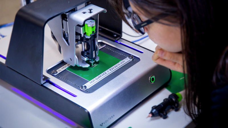
Voltera Unlocks Democratization
Canada-based Voltera is one of the companies leading the development of accessible printing solutions for electronic prototyping. To date, the company has released two benchtop printing systems, the V-One and the NOVA both of which are used by product developers and educators all over the world. The company’s technologies are central to its mission to make electronic design tools more accessible to unlock greater innovation in the field. Ultimately its aim is to catalyze innovation by removing barriers to entry.
V-One: A tool for all
Voltera’s first system, the V-One, is a desktop PCB printer that combines multiple functionalities into a single intuitive platform. These functionalities include everything you need to rapidly prototype a printed circuit board, from circuit printing and through-hole drilling, to solder paste dispensing and reflow soldering. Available for less than $6,000, the V-One makes it possible to print and assemble PCBs in just an hour and, notably, allows all scales of user to bring prototyping in house. This ultimately enables users to accelerate lead times dramatically and retain control over their intellectual property (IP).
NOVA: Advanced capabilities for the masses
Voltera’s second system is NOVA, an inkjet-based electronic printer that is capable of printing a broad range of conductive and dielectric inks onto a variety of substrates, including those made from rigid materials and flexible materials. The benchtop system, which is controlled via an intuitive browser-based app, enables the production of highly complex electronics without the need for ultra-sophisticated technologies and prohibitively expensive infrastructure. This means that Voltera customers have the freedom to experiment and innovate as they develop new devices without the time lags and costs associated with more conventional prototyping approaches.
Democratization of Electronic Design at Work
There are already several examples of Voltera’s platforms being used to develop innovative devices and projects by all types of adopters, from educational institutions, to startups and innovators, to those in regions with limited resources. Below are just a few case studies that illustrate the technology’s potential.
Small spacecraft
Students in Princeton University’s Mechanical and Aerospace Engineering Department are leveraging the V-One system to design functional devices, like CubeSats and other small spacecraft, for launch into space.[3] For undergrad students, tools like the V-One are making all the difference in turning more theoretical exercises into a tangible reality. Notably, the prototyping system gives students a deeper understanding of PCB production since they are working with the technology first hand, rather than sending a design out for production. Mike Galvin, Sr Tech Support, Mechanical Engineer at Princeton University, said of the project: “Before [the students] graduate they can see a small spacecraft through from conceptual design, through preliminary design review, through detailed design, integration, build, fabrication, all the way through spacecraft qualification tests, integration for launch and finally orbital launch.”
Circuit Launch
Circuit Launch is a coworking startup for hardware entrepreneurs that houses a wide range of prototyping and production systems in house, including the V-One.[4] The aim of Circuit Launch is to provide a space for individual innovators and small startups to both develop their products using cutting edge technologies and share ideas and skills. Having the V-One PCB printer in house enables Circuit Launch entrepreneurs to dramatically speed up development times for their respective products. “The Voltera V-One has been pushing our entrepreneurs to create new things in a faster and more economical way than almost any of our other machines,” said Dan O’Mara, Chief Operating Officer of Circuit Launch.
Biomedical tattoos
Yoland El-Hajj, a student in at York University, is developing printed biomedical tattoos for electrophysiological signal acquisition using Voltera’s NOVA platform.[5] Her research is based on the idea that conformal sensors placed on the body can provide more accurate electrophysiological readings compared to rigid sensors. As part of her work, El-Hajj is using the NOVA printer to iterate flexible “tattoos” embedded with electronic sensors that can be transferred onto the skin. The NOVA has enabled her to experiment with different sensor shapes and designs to evaluate which are the most effective and durable. Down the line, these printable biomedical tattoos could be used for ECG and EMG monitoring as well as to integrate prosthetics, and much more.
The Future Landscape of Electronics Design
With the continued emergence of user-friendly systems like Voltera’s V-One and NOVA, as well as growing adoption of these technologies, the accessibility of electronics design and development will continue to increase. Moreover, as a wider number of people gain access to the tools needed to develop new devices and products, the more innovation we will see, which in turn will further boost democratization. In other words, if you give more people the means to experiment and innovate, they will come up with original and potentially game-changing devices that could transform industries such as healthcare, transport, energy, and beyond.
References
[1] PCB Directory. “What is PCB Etching?” April 24, 2020. Available from: https://www.pcbdirectory.com/community/what-is-pcb-etching
[2] Wevolver. “Beyond Rigidity: The Rise of Flexible Electronics” December 8, 2023. Available from: https://www.wevolver.com/article/beyond-rigidity-the-rise-of-flexible-electronics
[3] Voltera. YouTube. “Voltera at Princeton University: The Future of Aerospace Innovation” Oct 2, 2019. Available from: https://www.youtube.com/watch?v=7TMoRObjmHI&t=3s
[4] Voltera. YouTube. “Voltera at Circuit Launch: Building Hardware Faster” Jan 8, 2019. Available from: https://www.youtube.com/watch?v=DqZHhqThCYU
[5] Voltera. YouTube. “NOVA at York University: Biomedical Tattoos” Sep 6, 2023. Available from: https://www.youtube.com/watch?v=MEW3q7GKYQA&t=1s