Transistor Circuit Design – Theory and Practice for Modern Engineers
This article explores transistor circuit design for digital design engineers, hardware engineers, and electronics engineering students. Find out the theoretical foundations with practical guidance, enabling you to confidently build and analyze analog and digital transistor circuits.

28 Jan, 2026. 14 minutes read
No time now? Save for later.
We only use your email to send this link. Privacy Policy.
Key Takeaways
Understanding transistor circuits, their operation regions, and characteristics is essential for both analog amplification and digital switching in modern electronic circuits.
Biasing and load‑line analysis are critical when designing BJT amplifier circuits, ensuring the transistor operates in the desired linear region for maximum signal swing.
MOSFETs are dominant in digital logic and power switching because they have high input impedance and operate efficiently in cut‑off and saturation regions. BJTs require base current and can suffer from crossover distortion in push‑pull stages.
Modern integrated circuits pack billions of transistors – Apple’s M3 Ultra contains 184 billion, Nvidia’s B100 GPU holds 208 billion, and wafer‑scale engines exceed four trillion – illustrating the scale and importance of transistor circuit design today.
The global transistor market is growing rapidly; wide‑bandgap materials, the demand for electric vehicles, and AI/5G applications are driving innovations in transistor circuits and amplifying the need for competent designers.
Introduction
Transistor circuits are found virtually in every electronic system, from smartphone processors to industrial power drives. From a designer’s perspective, transistor circuit design requires understanding transistor behavior under varying biasing conditions and integrating these devices into robust analog and digital designs. Digital design engineers, hardware engineers, and electronics engineering students often find themselves balancing theoretical principles with practical constraints such as power efficiency, thermal limits, and manufacturing costs. This article presents a comprehensive guide to transistor circuits, blending theory with real‑world examples and including current market data to show the importance of this field.
This article will explore how various transistor types function, how they behave in different operating regions, and how they are employed in amplifiers, logic gates, power switches, and current mirrors. We also explore design considerations such as bias stability, thermal management, and simulation techniques. Whether you are designing a high‑speed microprocessor or a simple sensor interface, this guide will clarify how to approach transistor circuits effectively.
Suggested Reading: Understanding Transistors: What They Are and How They Work
Basics of Transistor Circuits
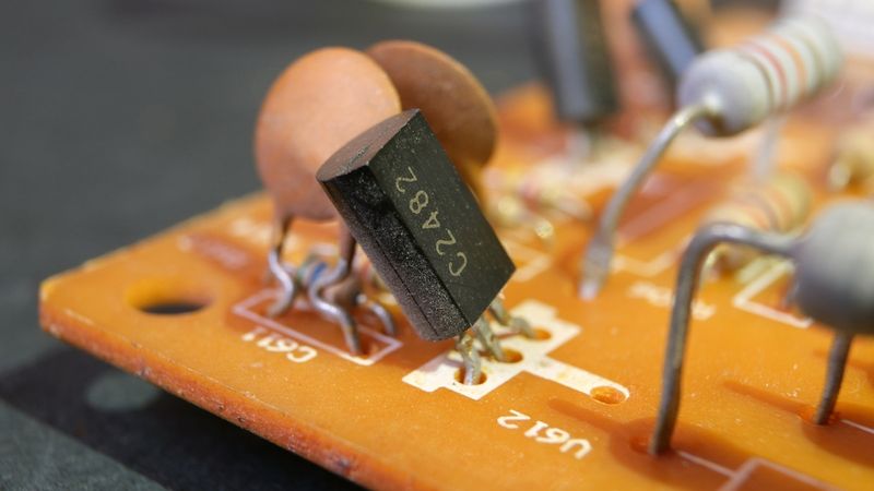
Transistor circuits are any electrical circuits in which one or more transistors control current or voltage. At its core, a transistor is a semiconductor device made of doped regions that can amplify signals or act as a switch.
Transistors are categorized into:
Bipolar junction transistors (BJTs)
Field‑effect transistors (FETs) including MOSFETs (metal–oxide–semiconductor FETs).
Although the basic role of controlling current is common, each type has distinct behaviors, advantages, and design considerations.
What Is a Transistor?
A transistor consists of three terminals. In a BJT, these are the emitter, base, and collector; in a MOSFET, they are the source, gate, and drain. A BJT relies on current injection into the base to control the collector–emitter current.
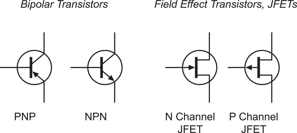
BJTs come in NPN and PNP polarities, determined by the ordering of n‑ and p‑type semiconductor layers. The primary performance metric is current gain β, defined as the ratio of collector current to base current.
A MOSFET, in contrast, uses an electric field to modulate the conductivity of a channel between source and drain. A gate insulated by an oxide layer controls the channel; there is no steady-state gate current, so MOSFETs have extremely high input impedance. MOSFETs can be n‑channel (electron conduction) or p‑channel (hole conduction).
MOSFET characteristics are described by threshold voltage Vth and on‑resistance RDSon. MOSFETs dominate digital electronic circuits because they consume little gate current and can be scaled down aggressively.
Suggested Reading: MOSFET Symbol: Theory, Practical Usage and Future Trends
Operating Regions and Modes
Understanding the operating regions of a transistor is crucial for designing reliable transistor circuits. For BJTs, the key regions are:
Operating region | Base–emitter (or gate–source) conditions | Collector–emitter (or drain–source) behavior | Application |
Cut‑off | For BJTs, the base–emitter junction is reverse-biased; for MOSFETs, Vgs is below Vth. | The collector (drain) current is essentially zero. | The transistor acts like an open switch or high‑impedance load. |
Active/Linear (Forward‑active) | Base–emitter junction is forward biased; for MOSFETs, Vgs exceeds Vth, and Vds is small. | Collector current is proportional to base current; the MOSFET behaves as a resistor. | Used for amplification in analog circuits. |
Saturation | Both junctions are forward-biased for BJTs. | Collector (or drain) current reaches its maximum and is relatively independent of base or gate voltage. | Used when transistors operate as switches. |
Reverse active and breakdown | Reverse active occurs when the collector–base junction is forward biased; breakdown happens when junction voltages exceed safe limits. | The device suffers from degraded gain and possible damage. | Typically avoided in standard operation. |
Transistors as the Building Blocks of Electronics
Transistor circuits serve two primary roles: amplification and switching. In the analog domain, amplifiers boost weak signals, as seen in audio equipment and sensor interfaces.
Digital systems rely on transistors as switches; logic levels correspond to on and off states. Complementary MOS (CMOS) logic uses pairs of n‑MOS and p‑MOS transistors to implement gates that consume virtually no static power when idle.
The impact of transistor circuits is most visible in the exponential growth of transistor counts in microprocessors and memory devices. According to a recent report, Apple’s M3 Ultra processor contains 184 billion transistors, while Nvidia’s B100 GPU packs 208 billion.
The Cerebras WSE‑3 wafer‑scale engine pushes this scale to around four trillion transistors, illustrating how integration has advanced. Moore’s law – the observation that transistor density doubles roughly every two years – continues to shape the expectations of digital engineers.
Suggested Reading: Chips and Wafers: What's the Difference?
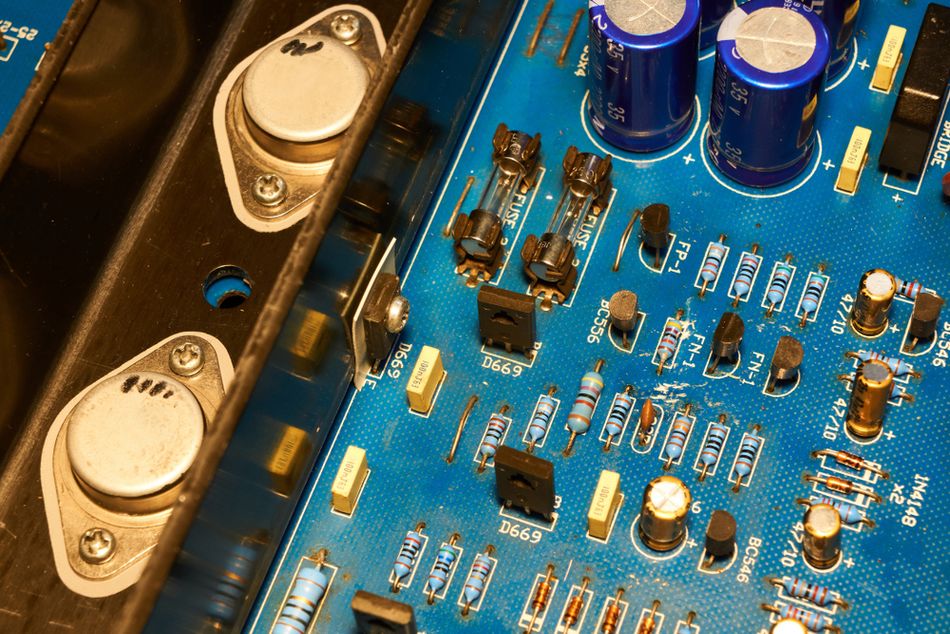
BJT Transistor Circuits
BJTs have long been the workhorse of analog design because they provide high transconductance and stable gain. BJTs are valuable in current mirrors, discrete amplifiers, and low‑power analog circuits. The following sections explore common BJT configurations and their design considerations.
Common‑Emitter Amplifier
The common‑emitter amplifier is a fundamental transistor circuit used to amplify small signals. In this configuration, the input is applied between base and emitter, the output is taken between collector and emitter, and the emitter is common to both input and output.
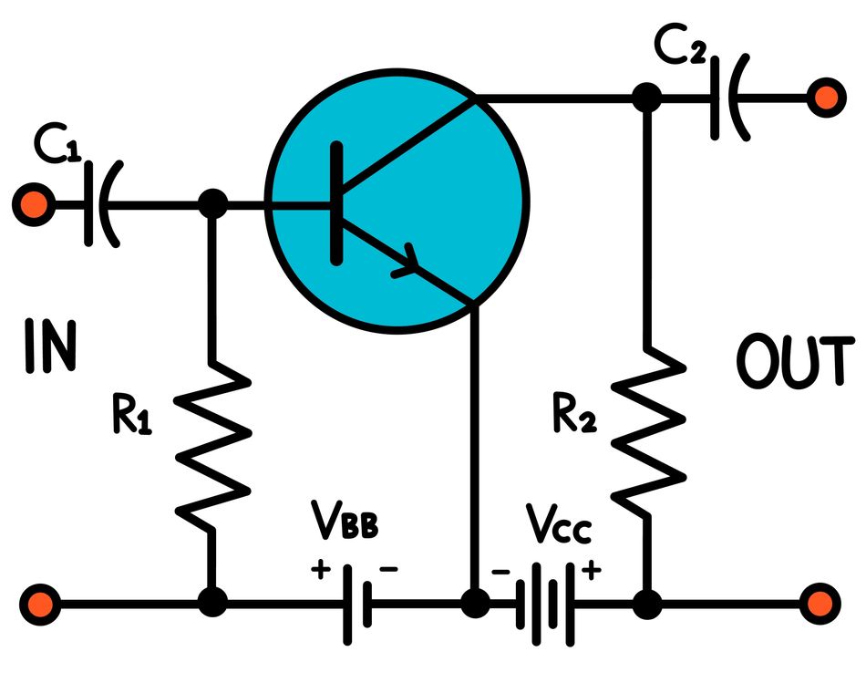
The key parameters for this configuration are voltage gain, input impedance, and output impedance. Proper biasing ensures that the transistor operates in the forward‑active region, where collector current is proportional to base current.
Biasing and Load‑Line Analysis
A stable operating point is achieved using bias networks, such as a voltage divider bias. The collector load line and the chosen Q‑point determine the maximum undistorted signal swing. The load line is drawn on the transistor’s output characteristic curves, and the intersection with the base bias line yields the operating point.
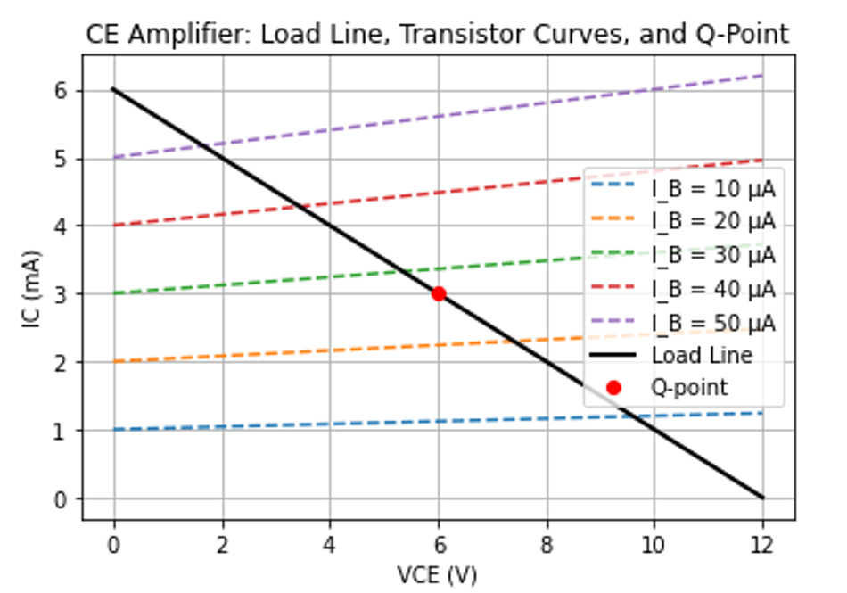
Selecting a Q‑point near the middle of the load line allows symmetrical voltage swing. A voltage divider across the supply sets the base voltage, while an emitter resistor provides negative feedback to stabilize the bias against transistor parameter variations.
Voltage Gain
The voltage gain of a common‑emitter amplifier is approximately -gm*Rc, where gm is the transconductance and Rc is the collector resistor. The negative sign indicates phase inversion. Bypass capacitors across the emitter resistor can increase AC gain by reducing AC feedback while maintaining DC stability.
Practical Tips
Choose the bias resistor values such that the base current is small relative to the current through the voltage divider, ensuring that the base voltage is relatively insensitive to β variations.
Include an emitter resistor to stabilize the operating point by providing local feedback; this resistor reduces gain slightly but improves linearity.
Use coupling capacitors at the input and output to block DC while allowing AC signals to pass; select values that provide low reactance at the lowest frequency of interest.
Push‑Pull Output Stage (Class B and AB)
High‑power audio amplifiers often employ a push‑pull output stage using a complementary pair of transistors. In a class B configuration, each transistor conducts for half of the input cycle. This arrangement offers high efficiency – around 78.5 % – but suffers from crossover distortion near the zero‑crossing point because of the transistors’ base–emitter threshold voltages.
To mitigate distortion, designers bias each transistor slightly on in class AB operation; this reduces crossover distortion at the cost of increased idle current.
A typical push‑pull stage uses an NPN and PNP transistor (or complementary MOSFET pair). The output is taken from the emitters (or sources). Diodes or biasing networks between the bases provide the correct forward bias to reduce crossover distortion.
BJT Switching Circuits
In digital and power electronics, transistors are frequently used as switches. An NPN transistor configured as a low‑side switch drives a load connected to the supply voltage. When the base voltage exceeds a threshold (approximately 0.7 V for silicon BJTs), the transistor enters saturation and behaves like a closed switch.
In the cut‑off region, the collector current is almost zero, while in saturation, both the base–emitter and base–collector junctions are forward biased, causing the collector voltage to drop close to the emitter voltage.
Designing a BJT Switch:
Determine the required collector current based on the load. Suppose the load draws 100 mA at 5 V.
Choose a transistor with sufficient current gain β and saturation current rating. Suppose β is 100.
Calculate base current: I<sub>B</sub> = I<sub>C</sub> / β = 100 mA / 100 = 1 mA. It is common to overdrive the base to ensure saturation, so you might design for 2 mA.
Set base resistor: If the driving logic output is 5 V and base–emitter voltage is 0.7 V, the base resistor is R<sub>B</sub> = (5 V – 0.7 V) / 2 mA ≈ 2.15 kΩ. Choose a standard value such as 2.2 kΩ.
Add a flyback diode across inductive loads (e.g., relays or motors) to protect the transistor from voltage spikes when the current is switched off.
Using a transistor in saturation reduces voltage drop across the device and minimizes power dissipation, making BJTs suitable for low‑to‑moderate power switching. However, MOSFETs often offer lower on‑resistance and are preferred in high‑current applications.
Recommended Reading: Transistor as a Switch: Theory and Practical Implementation for Digital and Hardware Engineers
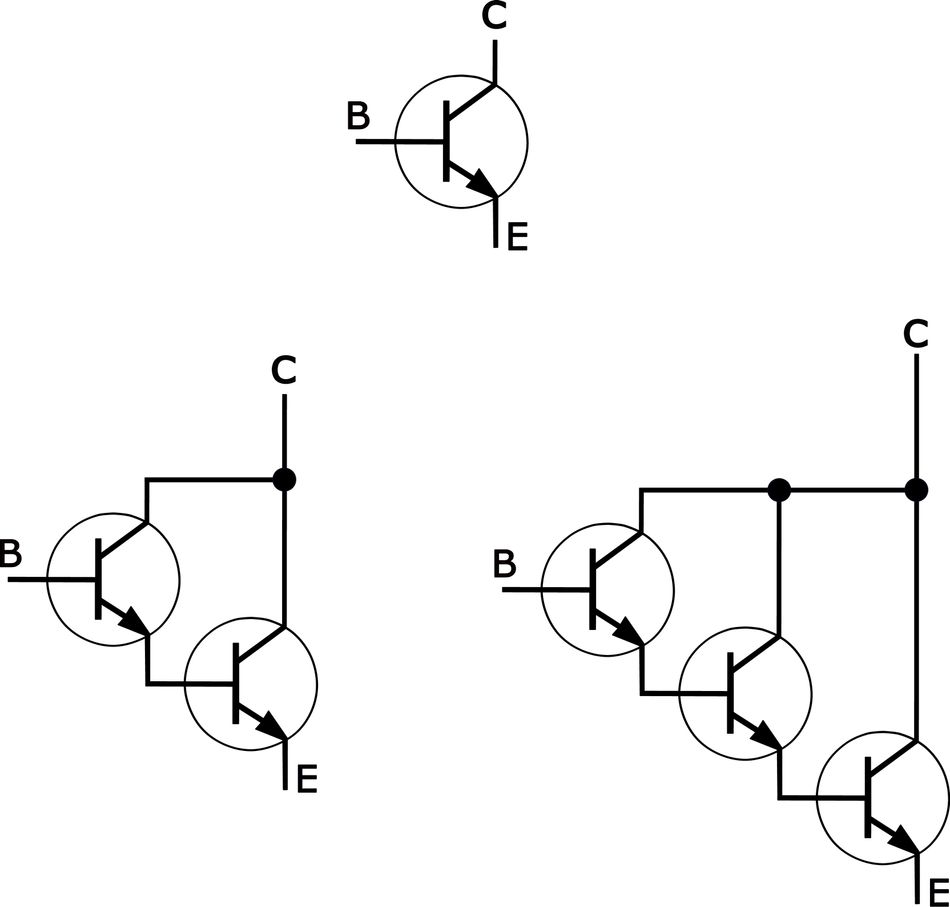
Darlington Pair and Current Mirror Circuits
When a single transistor cannot provide enough current gain, designers use a Darlington pair, which connects two transistors such that the emitter of the first drives the base of the second. This configuration produces a current gain equal to the product of the individual gains.
The emitter follower arrangement offers high input impedance and large current gain. The Darlington pair yields a high overall gain while maintaining simple biasing. A drawback is that the effective base–emitter voltage is the sum of two Vbe drops (≈1.2–1.4 V), which might require a higher input voltage.
Another important building block is the current mirror, which copies a reference current through one transistor to another identical transistor. A basic BJT current mirror uses two transistors: one is diode‑connected (base and collector shorted) to set the base–emitter voltage, while the other transistor, matched and connected with common base, replicates the collector current.
The current mirror provides stable bias currents and acts as an active load in amplifiers. CMOS current mirrors are also widely used in analog integrated circuits.
MOSFET and FET Transistor Circuits
The field‑effect transistor family includes MOSFETs, JFETs, and other insulated‑gate devices. MOSFETs dominate because they are easily integrated and have high switching efficiency. MOSFET circuits play critical roles in digital logic, power supplies, and RF amplifiers.
MOSFET Operating Modes
MOSFETs exhibit three principal operating modes:
Cut‑off: Vgs is below the threshold voltage Vth. The channel is off and only leakage current flows.
Triode or Linear Region: Vgs exceeds Vth and Vds is less than Vgs − Vth. The MOSFET behaves like a variable resistor. This region is used for analog applications and as a saturating load.
Saturation (Active) Region: Vgs exceeds Vth and Vds is greater than Vgs − Vth. The channel is pinched off, and the drain current is relatively independent of Vds. This region is used for amplification or as a constant‑current source.
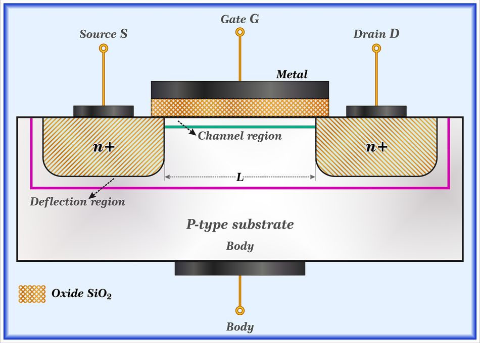
The drain current depends on threshold voltage and mobility; designers must account for variations due to process and temperature. Unlike BJTs, MOSFETs have a body diode inherent to their structure, which conducts when the drain–source voltage is reversed. This diode is beneficial in synchronous rectification but can cause unwanted conduction in certain circuits.
Suggested Reading: Rectifier Diode: Revolutionizing Electrical Applications with Advanced Semiconductor Technology
MOSFET as a Switch
MOSFETs are the preferred choice for high‑speed and high‑current switching because they have low on‑resistance and require no steady gate current. An N‑channel MOSFET used as a low‑side switch places the load between the supply and drain; the source is tied to ground. When the gate voltage rises above the source by more than Vth, the MOSFET turns on.
For high‑side switching a p‑channel MOSFET can be used with the source connected to the supply; it turns on when the gate voltage is lower than the source. Alternatively, a gate‑driver circuit using a bootstrap can drive an N‑channel MOSFET on the high side to achieve lower on‑resistance.
Key considerations when using MOSFETs as switches include:
Gate Drive Strength: Although no steady current flows into the gate, turning the device on and off requires charging and discharging the gate capacitance. A low‑impedance driver reduces switching losses and shortens transition times.
Rdson: The on‑state resistance must be low to minimize conduction losses. Power MOSFETs specify Rdson at a given gate voltage.
Safe Operating Area: MOSFETs are sensitive to overvoltage. Avalanche ratings and transient‑voltage‑suppressor diodes protect against voltage spikes.
Body Diode: When switching inductive loads, the intrinsic diode can either conduct the flyback current or cause losses; an external diode or synchronous rectification may be necessary.
Power MOSFET Design and Applications
Power MOSFETs are optimized for high current and voltage applications. They use large channel widths and cell architectures such as trench gates to reduce R<sub>DS(on)</sub>. These devices enable efficient DC–DC converters, motor drives, and synchronous rectifiers. In switching power supplies, MOSFETs operate in a pulse‑width‑modulated regime, rapidly switching between cut‑off and saturation. Loss minimization requires balancing conduction and switching losses; selecting appropriate gate drivers and snubber networks is critical.
Advanced MOSFETs incorporate superjunction structures and wide‑bandgap materials like silicon carbide (SiC) and gallium nitride (GaN). These materials provide lower on‑resistance and higher breakdown voltages than silicon, enabling more efficient and compact power circuits. The growth in electric vehicle and renewable energy markets has accelerated the adoption of these devices.
Recommended Reading: How Do MOSFETs Work: Comprehensive Technical Guide for Engineers (2025)
Digital Logic and Integrated Circuits
Transistor circuits form the basis of digital logic. A logic gate is essentially a network of transistors configured to produce a logical output from defined inputs. CMOS logic, for instance, uses complementary n‑MOS and p‑MOS transistors to create gates that draw almost no current when static.
CMOS Logic Gates
In a CMOS inverter, an n‑MOS transistor pulls the output low when the input is high, and a p‑MOS transistor pulls the output high when the input is low. Because only one transistor conducts at a time, static power consumption is minimal.
Propagation delay and dynamic power are determined by the capacitive load and switching frequency. NAND, NOR, and XOR gates are created by arranging multiple transistors in series or parallel.
Latches, Flip‑Flops, and Memory
Sequential circuits such as latches and flip‑flops are built from cross‑coupled transistor pairs. A basic SR latch uses two cross‑connected NOR or NAND gates; more complex devices like D flip‑flops add clock inputs to control when state changes occur.
At larger scales, transistor circuits form static and dynamic RAM cells, with SRAM using cross‑coupled inverters and pass transistors to store bits. DRAM uses a single transistor and a capacitor per bit. In all cases, careful sizing of transistor dimensions and consideration of leakage currents determine performance and power consumption.
Suggested Reading: Mastering Flip-Flop Circuits: Theory, Design, Types, and Real-World Applications
System‑on‑Chip and Transistor Counts
Modern system‑on‑chip (SoC) designs integrate processors, memory, and analog interfaces on a single die. The number of transistors in these designs has grown at an astonishing rate.
According to reports, Apple’s M3 Ultra contains 184 billion transistors, Nvidia’s B100 GPU has 208 billion, and the Cerebras WSE‑3 wafer-scale engine boasts around 4 trillion transistors. Even memory devices show staggering numbers: a Samsung V‑NAND module contains 5.3 trillion transistors.
Practical Design Considerations
Transistor circuit design is not purely theoretical; numerous practical issues influence reliability and performance. This section provides guidelines to help engineers translate theory into robust hardware.
Biasing and Stability
Transistor parameters such as β, Vbe, and Vth vary with temperature and manufacturing tolerances. Bias networks must therefore provide stability. As described earlier, a voltage divider bias combined with an emitter resistor in a common‑emitter amplifier stabilizes the operating point against β variations.
Similarly, MOSFET gate bias circuits use resistor networks or constant‑current sources to set a stable Vgs. Feedback and degeneration resistors linearize the gain and reduce distortion.
When biasing transistor circuits, keep these practices in mind:
Use voltage feedback from the collector (or drain) to the base (or gate) through resistors to stabilize DC operating points.
Bypass capacitors on supply rails prevent oscillations and reduce power supply noise.
Thermal stability can be improved by mounting temperature‑sensitive components (e.g., bias diodes or transistors) close together so they track each other.
Simulation and Prototyping
Before building hardware, simulate transistor circuits using SPICE or other circuit simulators. Models incorporate device nonlinearities and parasitics. Simulations allow you to observe operating points, waveforms, and transient responses.
After simulation, build a prototype on a breadboard or PCB and measure voltages and currents to verify that real‑world behavior matches expectations. Pay attention to stray capacitances and inductances, as these can cause oscillations or degrade performance.
Market and Technology Trends
Understanding market trends informs design priorities. It has been reported that the global transistor market was valued at USD 18.63 billion in 2025 and is expected to grow to USD 28.66 billion by 2031.
BJTs accounted for about 48.35 % of the market in 2025, while silicon remained the dominant material with a 68.85 % share. Wide‑bandgap materials such as SiC and GaN are gaining traction due to their higher breakdown voltages and efficiency, particularly in electric vehicles and renewable energy systems. Demand for AI/ML acceleration, 5G/6G connectivity, and mobile SoCs is driving innovation and pushing transistor circuits toward greater integration and performance.
Conclusion
Transistor circuits are the foundation of modern electronics. This article has covered theoretical concepts – such as operating regions, biasing, and amplification – as well as practical implementations including switching circuits, current mirrors, and CMOS logic. Practical topics such as bias stability, thermal management, simulation, and market trends ensure that engineers can apply these insights to real designs.
New technologies like gate‑all‑around FETs, FinFETs, nanosheet transistors, and 2D materials promise further improvements in performance and scaling. The integration of wide‑bandgap semiconductors will continue to reduce losses in power electronics. As transistor counts soar into the trillions, engineers must confront challenges of interconnect delay, heat dissipation, and variability.
FAQs
What is the difference between a BJT and a MOSFET transistor circuit?
BJTs control current using a small base current; they are current‑controlled devices and exhibit significant gain, and are used in analog amplifiers. MOSFETs control current with a voltage applied to the gate, consuming negligible gate current, and are used in digital logic and power switching.
How do I calculate the base resistor for a transistor switch?
First determine the collector current required by the load. Divide this current by the transistor’s DC current gain (β) to estimate the base current. Multiply the base current by a safety factor (e.g., 2) to ensure saturation. Then compute the base resistor as (V- Vbe)/Ib. Choose a resistor with the nearest standard value. Use a flyback diode across inductive loads to protect the transistor.
What is the purpose of a current mirror in transistor circuits?
A current mirror copies a reference current through one transistor to one or more other transistors. It provides precise bias currents and acts as an active load in differential amplifiers. A basic BJT current mirror uses a diode‑connected transistor to set the base–emitter voltage and a matched transistor to mirror the current.
How do transistor counts influence digital chip performance?
Higher transistor counts allow for more complex logic, larger caches, and improved parallelism. Apple’s M3 Ultra with 184 billion transistors and Nvidia’s B100 with 208 billion demonstrate the capacity to integrate multiple processing cores, memory, and accelerators on a single die.
What are the major trends in transistor technology?
Important trends include the shift toward wide‑bandgap materials like SiC and GaN for power electronics, the adoption of FinFETs and gate‑all‑around FETs in advanced CMOS nodes, and the exploration of 2D materials like graphene for future devices. The global market for transistors is expected to grow significantly due to electric vehicles, artificial intelligence, and 5G/6G technologies.
References
Wikipedia, “Transistor count,” Wikipedia. [Online]. Available: https://en.wikipedia.org/wiki/Transistor_count
Apple, “Apple reveals M3 Ultra taking Apple silicon to a new extreme,” Apple Newsroom, Mar. 2025. [Online]. Available: https://www.apple.com/newsroom/2025/03/apple-reveals-m3-ultra-taking-apple-silicon-to-a-new-extreme/
Viperatech, “NVIDIA B100 Blackwell AI GPU,” Viperatech. [Online]. Available: https://viperatech.com/product/nvidia-b100-blackwell-ai-gpu
NVIDIA, “NVIDIA Blackwell platform arrives to power a new era of computing,” NVIDIA Newsroom. [Online]. Available: https://nvidianews.nvidia.com/news/nvidia-blackwell-platform-arrives-to-power-a-new-era-of-computing
Electronics Tutorials, “Common emitter amplifier and transistor amplifiers,” Electronics-Tutorials.ws. [Online]. Available: https://www.electronics-tutorials.ws/amplifier/amp_2.html
Electrical Technology, “Types of transistors - BJT, FET, JFET, MOSFET, IGBT & special transistors,” ElectricalTechnology.org, Aug. 2021. [Online]. Available: https://www.electricaltechnology.org/2021/08/transistor-types-of-transistors.html
Electronics Tutorials, “Class AB amplifier design and class AB biasing,” Electronics-Tutorials.ws. [Online]. Available: https://www.electronics-tutorials.ws/amplifier/class-ab-amplifier.html
Electronics Tutorials, “The MOSFET and metal oxide semiconductor tutorial,” Electronics-Tutorials.ws. [Online]. Available: https://www.electronics-tutorials.ws/transistor/tran_6.html
HIBIT, “Transistors: the building blocks of our digital world,” HIBIT.dev. [Online]. Available: https://www.hibit.dev/posts/116/transistors-the-building-blocks-of-our-digital-world
in this article
1. Key Takeaways2. Introduction3. Basics of Transistor Circuits4. BJT Transistor Circuits5. MOSFET and FET Transistor Circuits6. Digital Logic and Integrated Circuits7. Practical Design Considerations8. Conclusion9. FAQs10. ReferencesNo time now? Save for later.
We only use your email to send this link. Privacy Policy.