Mastering Flip-Flop Circuits: Theory, Design, Types, and Real-World Applications
A comprehensive technical guide to flip-flop circuits for digital designers and hardware engineers. Learn the core theory behind latches and flip-flops, explore SR, D, JK, and T types, master critical timing concepts, and apply practical design strategies through real-world examples.

17 Dec, 2025. 18 minutes read
Key Takeaways
- Bistable Storage Element: Flip-flops are edge-triggered bistable devices used in digital logic and electronic circuits that store one bit of information and update their state only on clock events, ensuring predictable functionality in synchronous circuitry [1] .
- Flip-Flop Variants: SR, D, JK, and T flip-flops implement different input signals, with the JK flip-flop capable of emulating all others through appropriate input tie-offs.
- Timing Requirements: Reliable flip-flop operation depends on meeting setup, hold, recovery, and removal timing constraints. These parameters are critical when analyzing a circuit diagram and validating timing using static timing an,alysis and delay-based models.
- Metastability Behavior: Metastability occurs when data and clock transitions violate timing windows, potentially causing temporarily unstable or indeterminate states, and is mitigated through synchronizer chains and proper timing margin [1].
- Implementation Considerations: Practical flip-flop implementations vary across logic families such as CMOS and TTL. Designers must consider propagation delay, power consumption, asynchronous set/reset behavior, and underlying circuitry, including gates, transistors, and supporting components such as diodes.
Introduction
In digital systems, information is represented using two states: 0 and 1. Basic electronic circuits, called combinational circuits, like AND, OR, and NOT gates, produce outputs based only on the current input signals. But most real-world digital systems need a way to store information and remember past states.
This is where sequential circuits come in. Unlike combinational circuitry, sequential circuits can store and use previous information, allowing systems to keep track of events over time. This ability to “remember” is crucial for building registers, counters, memory units, pipelines, and state machines, enabling computers and digital systems to perform complex tasks reliably and predictably. A key building block in sequential circuits is the flip-flop. Flip-flop circuits are clocked electronic circuits that store one bit of information and change their state in a controlled way, usually synchronized with a clock signal. They form the backbone of memory and timing in digital systems. Understanding the operation of flip-flop circuits is fundamental for designing synchronous systems such as microprocessors, FPGAs, and ASICs.
This article explains the theory of flip-flop circuits, contrasts them with latches, explores common types (SR, JK, T, and D type flip-flops), and offers guidelines for practical implementation.
What Are Flip-Flops?
A flip-flop is a fundamental building block in digital electronics that can store a single bit of information—either a 0 or a 1. Unlike simple logic gates, which output a result immediately based on current inputs, flip-flops can remember a previous state until they are triggered to change. This “memory” property makes them essential for sequential circuits, where the output depends not only on current inputs but also on past inputs.
Flip-flops have two main outputs:
Q – represents the stored bit
Q′ (Q bar) – the complement of Q
Most flip-flops are synchronized with a clock signal, meaning they change their state only at a specific moment in time (such as the rising or falling edge of the clock). This allows digital systems to operate in a coordinated and predictable way, avoiding errors that can occur if signals change unpredictably.
Flip-Flops vs Latch
While both latches and flip-flops are bistable memory elements capable of storing a single bit, they differ in how and when they change their state:
Latches are level-sensitive, meaning they respond to input changes whenever the enable signal is active. For example, if a latch is enabled and the input changes, the output immediately follows the input. This makes latches fast and simple, but it also introduces a potential problem called transparency. During the time the latch is enabled, any unintended changes in the input can propagate to the output, causing glitches or timing errors. Because of this, latches are generally used in asynchronous circuits or in specific low-power designs where careful timing control is possible.
Flip-flops, on the other hand, are edge-triggered, meaning they update their output only at a specific transition of a clock signal—either the rising edge (low to high) or falling edge (high to low). This makes flip-flops synchronous devices, as all flip-flops in a system can be coordinated by the same clock. Edge triggering prevents the transparency problem of latches, allowing outputs to remain stable except at the precise clock moment. This precise timing is essential for reliable sequential circuits, including registers, counters, pipelines, memory arrays, and finite state machines.
In short, while latches are useful for simple or low-power applications, flip-flops are the preferred building blocks in most synchronous digital systems because they provide controlled, predictable behavior, making the design of complex circuits much easier and more robust.
Types of Flip-Flops
Digital systems use several standard types of flip-flops, each defined by how its inputs control the next output state. Although every flip-flop stores only one bit, different designs offer different behaviors—such as simple storage, toggling, or controlled setting and resetting. The four most commonly used types in synchronous digital design are:
SR (Set–Reset) Flip-Flop
D (Data) Flip-Flop
JK Flip-Flop
T (Toggle) Flip-Flop
SR (Set‑Reset) Flip Flop
The SR flip-flop, also known as the Set-Reset flip-flop, is the simplest type of flip-flop [2]. It is derived from the SR latch but includes a clock input to control when the state can change. Its primary purpose is to store a single bit of information while allowing controlled setting or resetting of that bit.
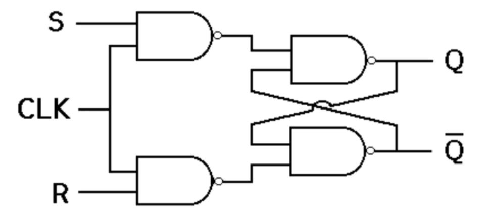
The SR flip-flop has two inputs, S (set) and R (reset), two outputs Q and Q′, and a clock signal (Clk). It has two complementary outputs: Q, which represents the stored bit, and Q’ (or Q-bar), which is the inverse of Q. The clock input ensures that changes to Q occur only at the designated clock transition, preventing glitches caused by unintended input changes. When a positive clock edge arrives, the flip-flop evaluates the S and R inputs and updates the outputs accordingly.
Truth Table
S | R | Q(t) (current state) | Q(t+1) (next state) | Description |
0 | 0 | Q | Q | Hold state |
0 | 1 | X | 0 | Reset |
1 | 0 | X | 1 | Set |
1 | 1 | X | — | Forbidden |
- Hold state (S=0, R=0): The flip-flop retains its previous state.
- Set (S=1, R=0): The output Q becomes 1.
- Reset (S=0, R=1): The output Q becomes 0.
- Forbidden (S=1, R=1): This combination is invalid because it forces both outputs high, breaking the Q/Q’ complement rule. Designers must avoid this condition [2].
Characteristic Equation
The next-state logic of the SR flip-flop can be expressed as:
Qₙ₊₁ = S + Qₙ·R̄
This equation captures the essential behavior: Q is set when S=1, reset when R=1, and holds when both are 0.
SR flip-flops are commonly implemented using cross-coupled NOR or NAND gates. To make them edge-triggered, gating circuits are added to allow S and R to affect the outputs only at the clock edge. While simple, the SR flip-flop is rarely used in modern designs because the forbidden input combination (S=R=1) can cause unpredictable behavior. Designers typically prefer D or JK flip-flops, which eliminate this ambiguity.
Applications
Despite its limitations, the SR flip-flop is useful for:
Basic memory storage in small circuits.
Latching a control signal to maintain a state until explicitly changed.
For educational purposes and introductory tutorials.
D (Data) Flip Flop
The D flip-flop, also called the Data or Delay flip-flop, is one of the most widely used flip-flop types in digital electronics. Its primary function is to capture the value of a single data input (D) at a specific clock pulse and hold it until the next clock event. Unlike the SR flip-flop, the D flip-flop has only one data input, which eliminates the possibility of invalid input states and simplifies design. This makes it ideal for use in registers, shift registers, and synchronous memory circuits.
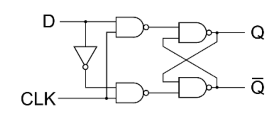
A standard D flip-flop has a data input (D), a clock input (Clk), and two outputs: Q (the stored bit) and Q’ (the complement). Optional asynchronous set and reset inputs are often provided to initialize or force the flip-flop state regardless of the clock. The key feature is edge-triggering: the flip-flop samples the D input only at the rising (or falling) edge of the clock, ensuring stable and predictable data storage.
Recommended Reading: FPGA Programming: Theory, Workflow, and Practical Implementations
Truth Table
The D flip-flop’s behaviour can be summarised in a concise truth table:
Clock | D | Q(t+1) | Description |
Rising edge | 0 | 0 | Store 0 |
Rising edge | 1 | 1 | Store 1 |
Other times | X | Q | Hold state |
On the active clock edge, the Q output takes the value of the D input.
At all other times, the output holds its previous state.
Asynchronous set/reset inputs, if used, override the D input to force Q=1 or Q=0, respectively.
Characteristic Equation
The behavior of the D flip-flop can be expressed simply as:
Qₙ₊₁ = D
This equation shows that the next state of the flip-flop is always equal to the current value of the D input at the clock edge.
There are various implementations of D flip-flops. A classical positive‑edge‑triggered D flip-flop consists of two SR latches arranged in a master–slave configuration: the first (master) latch captures the D input when the clock is low, and the second (slave) latch transfers the master’s output to Q when the clock goes high [1]. Depending on the target technology, the internal latches of a D flip-flop may be implemented using NOR gate–based or NAND-based circuitry, with the choice influencing noise margins and switching behavior. This arrangement ensures that the output changes only at the clock edge and not in the middle of the cycle.
A master–slave flip flop can also be triggered on the falling edge by inverting the clock to the first latch; dual‑edge‑triggered designs capture input data on both rising and falling edges and can be built using two single‑edge‑triggered D flip-flops with a multiplexer or XOR gates. High‑speed circuits often use dynamic D storage elements, where information is stored on capacitances; these circuits have low power consumption but may suffer from leakage at low frequencies.
D flip-flops are widely available in CMOS and TTL logic families. They are highly reliable for synchronous designs because they eliminate the forbidden input states present in SR flip-flops.
Applications
Data storage and transfer: Holding bits in registers or pipelines.
Shift registers: Serial-to-parallel or parallel-to-serial conversion.
Counters and finite state machines: Storing state information.
Clocked memory elements in FPGAs and ASICs: Reliable synchronization in synchronous digital systems.
JK Flip Flop
The JK flip-flop is a versatile and widely used type of flip-flop that builds on the limitations of the SR flip-flop. While the SR flip-flop has an invalid input condition (S=1 and R=1), the JK flip-flop eliminates this issue by redefining the behavior of the “both inputs high” case. In the JK design, when both inputs J=1 and K=1, the flip-flop toggles, meaning the output switches to the opposite state at the active clock edge. This makes the JK flip-flop more flexible and suitable for counters, frequency division, and control circuits.
A JK flip-flop has two data inputs: J (set-like input) and K (reset-like input), one clock input, and two outputs Q and Q’. Like other synchronous flip-flops, the JK flip-flop updates its output only at the clock’s rising or falling edge, depending on the design. Optional asynchronous preset and clear inputs may be included to force the output high or low, independent of the clock.
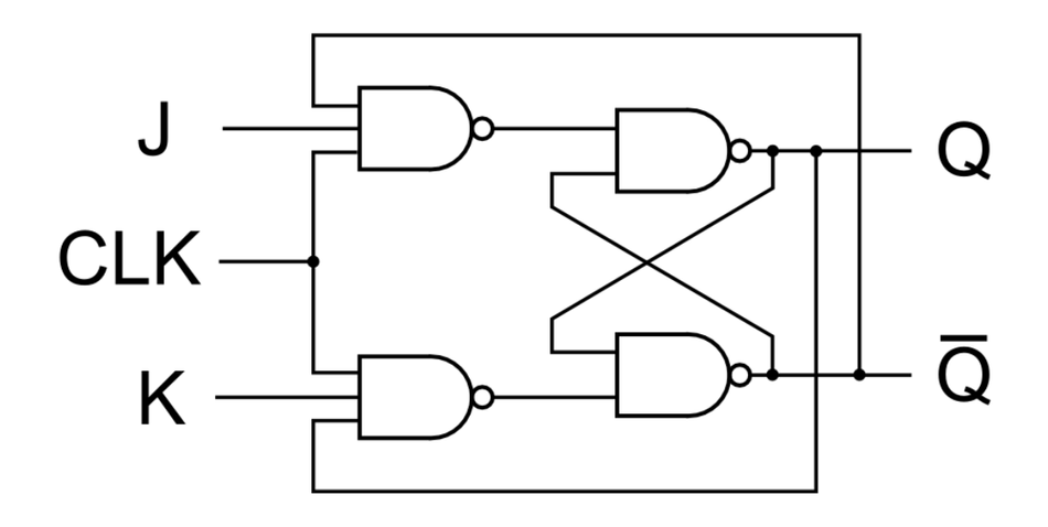
What makes the JK flip-flop unique is its feedback mechanism: the current output Q is fed back into the input logic, allowing the flip-flop to toggle and preventing the invalid condition present in SR designs.
Truth Table
The truth table derived from this equation is summarised below:
J | K | Q(t) | Q(t+1) | Description |
0 | 0 | Q | Q | Hold state |
0 | 1 | X | 0 | Reset |
1 | 0 | X | 1 | Set |
1 | 1 | Q | ¯Q | Toggle (complement) |
Hold (J=0, K=0): The flip-flop retains its current state.
Set (J=1, K=0): The output becomes 1.
Reset (J=0, K=1): The output becomes 0.
Toggle (J=1, K=1): The output flips its value on each clock edge.
Characteristic Equation
The characteristic equation of the JK flip-flop is:
Qₙ₊₁ = J·Q̄ₙ + K̄·Qₙ
The JK flip-flop’s toggle mode is widely used to divide clock frequencies by two. For example, if a T input is connected by tying J and K together, the JK flip-flop becomes a T flip-flop (described below) and toggles its output on each clock edge, effectively halving the input frequency.
A typical JK flip-flop uses two 3‑input AND gates feeding into an SR latch. The outputs Q and Q′ feed back to the AND gates to inhibit further state changes until the next clock edge. The cross‑coupled feedback ensures that the J=K=1 condition toggles the output rather than causing an illegal state. Because JK flip-flops require more gates than D flip-flops, they consume more power and area, but their universality and toggling ability make them suitable for counters and frequency division.
Applications
The JK flip-flop’s versatility makes it popular in:
Binary counters (e.g., ripple or synchronous counters)
Frequency dividers (toggle mode divides clock by 2)
Control systems and state machines
Universal flip-flop configurations, since JK inputs can be tied together to create a T flip-flop or wired to emulate a D flip-flop
Because it can emulate SR, D, and T flip-flops through wiring changes, the JK flip-flop is often referred to as a universal flip-flop.
T (Toggle) Flip Flop
The T flip-flop, short for Toggle flip-flop, is a simplified and specialized flip-flop derived from the JK flip-flop [4]. It has only one data input, T, and its primary function is to toggle the output state whenever T=1 at the active clock edge. If T=0, the flip-flop holds its previous state. The T flip-flop is widely used in counters, frequency dividers, and sequencing circuits where periodic switching is required. It is one of the easiest flip-flops to understand conceptually:
T=1 → Change the output
T=0 → Keep the current output
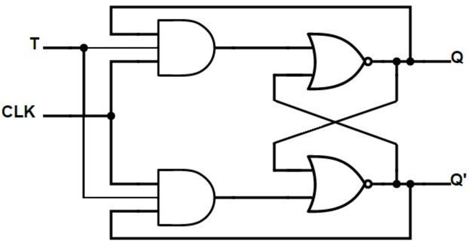
A standard T flip-flop includes a T input, a clock input (Clk), and the outputs Q and Q’. Like other synchronous flip-flops, it responds only at the clock edge, ensuring predictable and coordinated behavior within a synchronous system. Many commercial versions also include asynchronous set and reset pins for initialization or forced control of the stored bit.
The T flip-flop can be built directly or derived from other flip-flop types. The most common implementation ties the J and K inputs of a JK flip-flop together to form the single T input, simplifying the toggle mechanism.
Truth Table
The truth table appears below:
T | Q(t) | Q(t+1) | Comment |
0 | 0 | 0 | Hold |
0 | 1 | 1 | Hold |
1 | 0 | 1 | Toggle |
1 | 1 | 0 | Toggle |
Characteristic Equation
The characteristic equation of the T flip-flop is given below:
Qₙ₊₁ = T̄·Qₙ + T·Q̄ₙ
This expresses the toggling action mathematically: when T=1, the next state is the complement of Q; when T=0, the next state equals Q.
There are two common ways to implement a T flip-flop:
Using a JK flip-flop:
Tie J = K = T. When T=1, J and K both become 1, causing the JK flip-flop to toggle.
When T=0, J=K=0, and the flip-flop holds its state.Using a D flip-flop:
Feed the XOR of T and Q into the D input: D = T ⊕ Q.
This ensures that the D flip-flop outputs a toggled value when T=1 and holds the value when T=0.
Both implementations preserve edge-triggered operation and ensure clean transitions controlled by the clock.
Applications
The T flip-flop is especially valuable in circuits requiring predictable toggling:
Binary counters: A chain of T flip-flops forms a ripple counter, where each flip-flop toggles based on the previous stage’s output.
Frequency division: When T=1, the flip-flop divides the clock frequency by 2, a fundamental function in digital timing systems.
State toggling/switching circuits: Useful for generating alternating patterns or stepping through binary sequences.
Control logic: Used in digital controllers where a periodic or alternating signal is required.
Because of its simplicity and predictable toggle behavior, the T flip-flop is a key building block in sequential digital systems.
Timing Parameters and Metastability
Setup Time and Hold Time
Flip-flop inputs must remain stable for a specific time window around the active clock edge to ensure correct sampling. This window is defined by two key parameters:
Setup time (Tsu): The minimum time before the clock edge during which the data input must remain stable.
Hold time (Thold): The minimum time after the clock edge during which the data input must remain stable.
Together, these form the sampling aperture of the flip-flop. If the data input transitions inside this window, the flip-flop may not reliably capture the intended value and can enter a metastable state.
Asynchronous set and reset inputs have their own timing requirements:
Recovery time: The asynchronous input must remain inactive for a minimum time before the clock edge.
Removal time: The asynchronous input must remain inactive for a minimum time after the clock edge.
Violating recovery or removal times can cause unpredictable results, including glitches or metastability.
Metastability
Metastability occurs when a flip-flop is asked to resolve an input change that happens too close to the clock edge. Instead of settling quickly to logic 0 or 1, the output may remain in an indeterminate analog level for an extended and unpredictable amount of time. In this state, the output may:
oscillate briefly,
take a long time to settle, or
resolve to an incorrect logic level.
In digital systems—especially those crossing clock domains—metastability can corrupt data, cause inconsistent states, or lead to intermittent and difficult-to-debug failures.
Metastability cannot be eliminated, but its probability can be reduced to extremely low levels using:
Proper timing closure (meeting setup and hold times),
Synchronizer chains (e.g., two or more cascaded flip-flops),
Clean asynchronous signal conditioning.
Propagation Delay and Timing Analysis
Propagation delay is the time required for a signal to travel from a source flip-flop to a destination flip-flop through combinational logic. Inside FPGAs or ASICs, signals travel through wires and logic gates. The further apart two flip-flops are, and the more logic is in between them, the longer the propagation delay. If the propagation delay exceeds the clock period, the design will fail to function properly. For example, if two flip-flops are 10 ns apart, a 50 MHz clock (20 ns period) leaves 10 ns of margin, whereas a 200 MHz clock (5 ns period) will fail timing.
A typical timing analysis involves checking:
Setup requirement: Tcq + Tpd + Tsu <= Tclk + Tskew
Hold requirement: T_cq + T_cd >= T_hold + T_skew
Where:
- Tcq = clock-to-Q delay
- Tpd = propagation delay through combinational logic
- Tcd = contamination delay
- Tclk = clock period
- Tskew = difference between clock arrival times at the two flip-flops
Real-world timing numbers often show that a path can meet setup timing with comfortable slack but still fail hold timing by a small margin—sometimes just a few picoseconds.
To correct timing issues, designers use techniques such as:
Pipelining – Breaking long combinational paths into multiple shorter stages using additional flip-flops.
Optimized placement and routing – Reducing wire delays.
Buffer insertion or delay balancing – Fixing hold violations by intentionally adding delay.
Controlled clock skew – Intentionally delaying or advancing clock edges when beneficial.
These strategies ensure reliable operation across all process, voltage, and temperature (PVT) variations.
Practical Implementation Considerations
Logic Families and Power Consumption
Flip flops can be implemented using different logic families such as TTL (transistor–transistor logic), CMOS (complementary metal–oxide–semiconductor), ECL (emitter‑coupled logic), and BiCMOS.
TTL (Transistor–Transistor Logic)
TTL flip-flops offer relatively fast switching with propagation delays typically in the 2–10 ns range and moderate power consumption in the milliwatt range. They were historically popular in early microprocessors and discrete logic systems.
CMOS (Complementary Metal–Oxide–Semiconductor)
CMOS flip-flops provide very low static power consumption, making them ideal for battery-powered and mobile devices. Dynamic D flip-flop designs exploit parasitic capacitances to store charge internally, enabling high performance with minimal energy usage.
ECL (Emitter-Coupled Logic)
ECL flip-flops achieve extremely high switching speeds—often sub-nanosecond delays—by operating transistors in their linear region. This comes at the cost of high static power consumption. ECL is used in ultra-high-speed communication, radar, and networking equipment. In TTL and ECL implementations, external resistors play an important role in setting logic levels, controlling current flow, and ensuring stable switching behavior.
BiCMOS
BiCMOS flip-flops combine bipolar junction transistors for fast switching and CMOS transistors for low power. This hybrid approach is used in high-speed digital and mixed-signal integrated circuits where both performance and power efficiency are critical.
In practice, the choice of flip-flop implementation depends on factors such as clock frequency, supply voltage, design constraints, available technology libraries, and power budget.
For example, a low-power microcontroller running at tens of MHz typically relies on CMOS D flip-flops, while multi-gigahertz SerDes and PHY interfaces may use current-mode logic (CML) or specialized high-speed flip-flop structures instead of standard CMOS cells.
Asynchronous Inputs and Glitch Suppression
Many commercial flip-flops provide asynchronous set (preset) and reset (clear) inputs. These inputs override the clock and force the output high or low. While useful for initialization, these inputs must be used carefully:
Designers must respect recovery and removal times so that asynchronous transitions do not interfere with the upcoming clock edge.
Very short pulses on asynchronous inputs can cause glitches or metastability if they occur during the recovery–removal window.
To avoid such issues, asynchronous signals are often filtered, synchronized, or stretched to guarantee clean transitions.
Clock Distribution and Skew
Clock skew refers to differences in clock arrival times at different flip-flops. It results from variations in routing length, buffer delays, loading, and manufacturing differences.
Positive skew: The capture clock arrives after the launch clock [3].
Negative skew: The capture clock arrives before the launch clock.
Designers manage skew by routing the clock through balanced trees (e.g., H‑trees), dedicated buffer networks, algorithmic clock tree synthesis (CTS), and inserting delay elements. Modern ASIC design tools perform clock tree synthesis to minimise skew.
Level‑sensitive versus Edge‑sensitive Design
While this article emphasises edge‑triggered flip-flops, level‑sensitive latches remain useful and are often used in:
Two-phase, non-overlapping clocking schemes,
High-performance pipelines,
Low-power circuits, where they reduce clock load,
Asynchronous or mixed-timing systems.
Because latches are transparent when enabled, they allow time borrowing, improving throughput by giving slow paths extra time as long as overall cycle constraints are met. However, they require careful control of clock phases and timing analysis to ensure that race conditions and unintended transparency do not occur.
Practical Uses of Flip-Flops in Electronics
Flip flops in FPGAs
In FPGAs, flip flops are embedded within configurable logic blocks (CLBs). Each flip-flop typically has a data input (D), clock input, optional enable, asynchronous set/reset, and sometimes clock enable. The propagation delay from the flip-flop output to the next flip-flop input depends on the routing and the look‑up table (LUT) configuration. When designing in hardware description languages (HDLs) such as Verilog or VHDL, synthesis tools map RTL descriptions—like always @(posedge clk) statements—to these hardware primitives. Best practice is to infer flip-flops in HDL rather than instantiate them directly, allowing the synthesis tools to optimize placement and timing for better performance.
Flip flops in System Design
Flip-flops serve as fundamental building blocks in higher-level modules:
Shift Registers: Chains of D flip-flops are used to transfer data serially or in parallel. For example, a serial-in parallel-out (SIPO) shift register shifts bits along the chain on each clock edge, enabling temporary data storage and serialization.
Counters: T flip-flops are commonly used in ripple counters to divide frequencies by powers of two. Synchronous counters can use T or JK flip-flops combined with combinational logic to produce arbitrary counting sequences.
Finite State Machines (FSMs): Flip-flops store the present state of the machine, while combinational logic determines the next state. The number of flip-flops required is typically the ceiling of log₂(number of states).
Frequency Dividers and Ring Oscillators: T flip-flops can divide a clock signal by two, four, or more, while rings of flip-flops or inverters with feedback can generate oscillatory signals for frequency synthesis or timing applications.
Debounce Circuits: Flip-flops help filter out mechanical switch bounces by sampling inputs only on clock edges, ignoring transient transitions and producing a clean, stable output.
These applications illustrate that flip-flops are not only memory elements but also versatile tools for timing, sequencing, and data management in digital electronics.
Design Guidelines and Best Practices
Avoiding Hazards and Races
Race conditions occur when signals with different propagation delays converge on a latch or flip- flop. In the SR latch, simultaneously de‑asserting both S and R can cause a critical race leading to an undefined next state. Designers avoid this by ensuring that S and R are never asserted or de‑asserted at the same time and by adding gating or edge-triggered flip-flops to eliminate transparency issues.
Ensuring Proper Input Conditioning
When connecting signals between different clock domains, use synchronizers—usually two flip flops in series—so that metastability decays before the signal is used in the new domain. Asynchronous or external signals should never be sampled directly without conditioning, as this greatly increases the risk of metastability. Do not sample asynchronous signals directly.
Meeting Setup and Hold Requirements
Use timing analysis tools to verify that every path between flip-flops meets setup and hold requirements. For failing paths, add pipeline stages, reduce combinational logic depth, optimize logic synthesis or adjust the clock frequency. For hold-time violations, buffers or intentional routing delays are commonly inserted to lengthen overly short paths, as demonstrated in timing-closure methodologies.
Considering Power and Area
Efficient design requires minimizing unnecessary flip-flops. Techniques such as optimized state-encoding (e.g., one-hot, binary, Gray) reduce storage requirements in FSMs. In ASICs, multi-bit flip-flops can significantly lower dynamic power by sharing clock drivers. In FPGAs, designers can take advantage of SRL (Shift Register LUT) primitives, which implement long shift registers more efficiently than chains of discrete flip-flops.
Testing and Verification
Simulate the design with realistic timing models, including specifications.
Conclusion
Flip-flop circuits are fundamental building blocks in synchronous digital design, providing deterministic state storage and enabling precise coordination of logic operations. Evolving from the basic bistable inverter pair, the family of SR, D, JK, and T flip-flops supports a wide range of functional behaviors suited to different architectural needs. The D flip-flop serves as the standard element for pipelines, registers, and FPGA logic, while JK and T devices offer powerful toggle and counting capabilities where appropriate. Ensuring reliable operation requires careful attention to setup and hold times, propagation delays, and the risk of metastability.
Through advanced timing analysis, pipelining, and clock-tree synthesis, modern design flows allow engineers to implement flip-flop-based circuits that maintain accuracy and stability even at high operating frequencies.
Frequently Asked Questions (FAQ)
What is the difference between a latch and a flip-flop?
A latch is level-triggered and changes state whenever its enable signal is active; whereas a flip-flop is edge-triggered and changes state only at a clock transition. Latches are asynchronous devices without an explicit clock, while flip-flops are synchronous devices with a clock.Why is the SR flip-flop seldom used in modern designs?
Because the input combination S=1 and R=1 results in both outputs going high, leading to an undefined state. The JK flip-flop solves this problem by interpreting J=K=1 as a toggle command.How does a master–slave D flip-flop work?
It cascades two latches controlled by inverted clock phases. The master latch captures the input when the clock is low, and the slave latch transfers the master’s output to Q when the clock goes high. This arrangement ensures that the output changes only on the clock edge.What causes metastability, and how can it be mitigated?
Metastability occurs when data and clock inputs to a flip-flop change too close together, causing the output to take an unbounded time to settle. Mitigation strategies include adhering to setup and hold times, using synchronizer chains, and designing for sufficient timing margin.What is propagation delay, and why is it important?
Propagation delay is the time a signal takes to travel from the output of one flip-flop to the input of another through combinational logic. If this delay plus setup time exceeds the clock period, the design will fail timing. Tools like static timing analysis help identify long propagation delays. Pipelining and logic optimization reduce propagation delay.How do setup and hold violations affect digital circuits?
If the data arrives too late (after the setup time), the flip-flop may capture incorrect data, causing functional errors. If the data changes too soon after the clock edge (violating hold time), metastability or glitches may occur [3].Can flip-flops operate on both rising and falling edges of the clock?
Yes. Dual-edge-triggered flip flops sample data on both the rising and falling edges. They can be implemented using two single-edge-triggered flip-flops and multiplexers or XOR gates. Dual-edge designs effectively double data throughput for a given clock frequency but require careful timing analysis.What is the advantage of the T flip-flop’s toggle function?
The toggle function allows the T flip-flop to divide the clock frequency by two when the T input is high, making it useful for counters, frequency division, and binary sequence generation.Why do designers prefer using D flip-flops in FPGAs?
FPGAs are built with logic cells that already contain a dedicated D-type register, so the hardware is optimized to accept a single data input and a clock. When designers write HDL, synthesis tools naturally map register assignments to these built-in D registers without requiring extra logic. In contrast, JK or T behavior does not exist as a native primitive and must be implemented using additional logic, which increases resource usage and complicates timing.What are the best practices for integrating asynchronous set/reset inputs?
Ensure that asynchronous inputs are inactive during the recovery and removal windows surrounding the clock edge. Use glitch filtering or synchronization circuits if these inputs originate from external asynchronous sources.
References
[1] Flip-flop (electronics), Wikipedia. Available: https://en.wikipedia.org/wiki/Flip-flop_(electronics). Accessed: Dec. 13, 2025.
[2] Latches and flip-flops, CS120B Digital Logic Course Notes, Univ. of California, Riverside. Available: https://www.cs.ucr.edu/~ehwang/courses/cs120b/flipflops.pdf. Accessed: Dec. 13, 2025.
[3] Setup Time, Hold Time, Contamination Delay & Clock Skew, JLCPCB Blog, Sept. 30, 2025. Available: https://jlcpcb.com/blog/digital-circuit-timing-setup-hold-contamination-delay-clock-skew. Accessed: Dec. 13, 2025.
[4] Flip-flops (JK, T, and master–slave description), CircuitVerse Documentation. Available: https://learn.circuitverse.org/docs/seq-ssi/flip-flops.html. Accessed: Dec. 13, 2025.