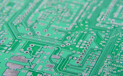
Filled vias are via holes that are completely filled and closed with conductive or non-conductive material or copper plating. The filled via is one of the many realizations of PCB via covering, specified by industry standards. This article covers the definition, benefits, processes, applications, and challenges of filled vias.
Technical Guides
Latest Posts
The most common plastic in the world, but can it be 3D printed? The answer is not as straightforward as you may think.
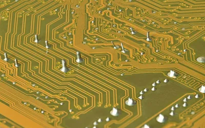
A cold solder joint is a defect caused by improper melting of solder to bond PCB electronic components. This defect can impact the functionality of a PCB assembly, and so must be carefully avoided.


The Creality Ender 3 and its V2/Pro variants have a stated print area of 220 x 220 mm, but the actual bed dimensions are 235 x 235 mm. So can you print right up to the edges or not?

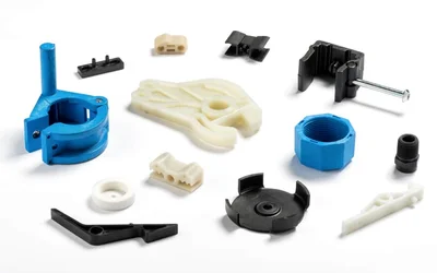
Most people consider 3D printing to be a prototyping process and injection molding to be a form of mass manufacturing. However, choosing between the two processes isn’t always straightforward.

Holonomic systems are important because they allow for efficient mathematical modeling and control of physical systems that have constraints on their motion.

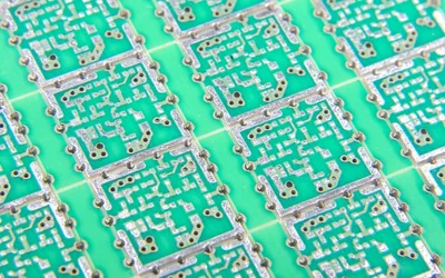
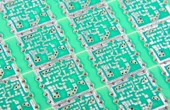
PCB Panelization is a PCB manufacturing technique. It involves the grouping of several small printed circuit boards to form a single array, which is known as a panel. Panelization is commonly employed in PCB manufacturing because it saves time and cost. This article discusses the conditions, design considerations, methods, types, and benefits of PCB panelization.
3D printing is creating new opportunities for injection molding, making low-volume production more viable than ever

Lead-free solders offer an environment-friendly alternative to toxic lead-based solders, which were dominant in the PCB manufacturing industry till the mid-2000s.


Here’s what you need to know about Delrin, a high-performance POM thermoplastic with exceptional strength, durability, and temperature resistance.

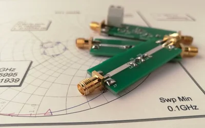
Controlled impedance in printed circuit boards involves the regulation of resistance exerted by signal traces. It is determined by characteristic factors of PCB fabrication, such as trace width and copper thickness. This article discusses controlled impedance and the essentials of its execution in PCB manufacturing.
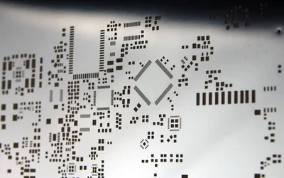
In this article, we will go over everything you need to know about PCB stencils.
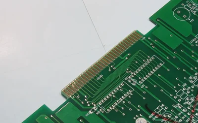
Approximately 7% of the world's gold can be found inside discarded electronic devices, in form of PCB Gold Fingers. While a tonne of Gold Ore produces just 5 grams of pure gold on average, a tonne of electronic scrap can house 300 grams of gold inside it. Here we gloss over the significance of gold fingers in the present day electronics industry and all kinds of gold fingers specifications you need to know.
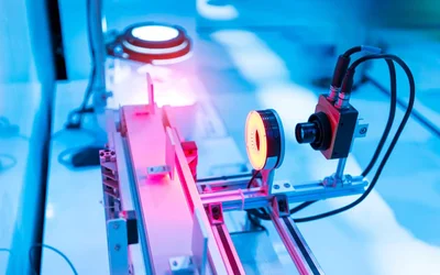
Sensors are used in robotics to calculate the condition and environment of robots, using functions similar to the human sensory organs. A variety of sensors are required by different robots to navigate their environment while performing tasks. This article covers the types of sensors in robotics.
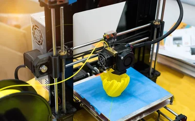
Understanding the differences and benefits of direct drive and bowden extrusion systems.
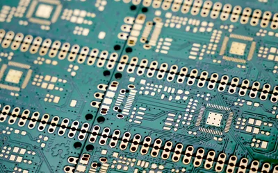
Vias go through two or more layers of PCBs to form an electrical connection. Making them right under the component’s pad saves space, reduces track inductance and simplifies design.

Marketing engineering products and services requires a strategic distribution of content in various forms. Using a combination of tech articles, e-books, newsletters, social posts, events, podcasts, and other sponsored content can significantly boost brand awareness.

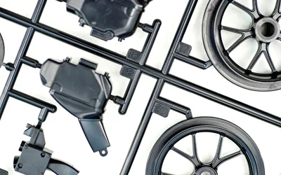
The sprues, runners, and gates of an injection mold are like the corridors and doorways between nozzle and mold cavity. So how exactly do they work?


HDPE can be found in objects like plastic bottles, garden chairs, and piping. But just how useful is HDPE filament for FDM 3D printing?


Beginners might be surprised to find that their 3D scans turn out not as solid 3D models, but as clusters of spatial data points. So what exactly is a point cloud, and what can you do with it?

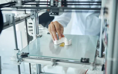
Good bed adhesion is key to achieving defect-free prints. But how do you remove 3D prints that are stuck firmly to the build surface of the 3D printer? This guide reveals all.
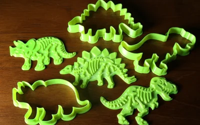
As a raw material, PETG is considered food-safe. However, the 3D printing process and filament brand can influence how food-safe it really is.
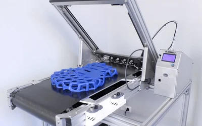
Conveyor belt 3D printers promise ultra-long parts and effortless batch printing. But are these hybrid FDM machines reliable enough for serious printing projects?
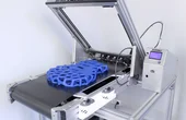
Wafer thinning is a part of the semiconductor manufacturing process. It is essentially grinding off the backside of the wafers to control their thickness and is useful for the production of ultra-thin wafers. These flattened wafers are used to effect stacked and high-density packaging in compact or microelectronic devices. This article discusses the meaning of wafer thinning, along with its various techniques and significance.
The rigid, flex and rigid-flex PCBs are all types of printed circuit boards. The rigid PCB is the traditional board and the base from which the other two variations came about, in response to industry and market needs. Flex PCBs introduced versatility to PCB fabrication and rigid-flex combines both for increased performance. Learn more about these board types, their benefits, disadvantages, and applications in this article.