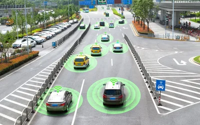
The automotive industry undergoes a profound transformation through the IoT's power. Vehicle connectivity and autonomous driving redefine transportation, offering innovative opportunities. Embracing IoT's potential, our daily lives are poised for a significant shift in the automotive sector.
Technical Guides
Latest Posts

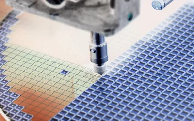
Silicon, with its abundant availability and unique properties, serves as the fundamental building block for semiconductor manufacturing. Its semi-metallic nature makes it an ideal material for controlled conduction of electricity. Furthermore, the combination of silicon with oxygen produces silicon dioxide, a crucial insulating component in silicon chip manufacturing.
This guide delves into DFM's principles, implementation process, impacts, and challenges, aiming to provide readers with a comprehensive understanding of this integral concept.
Die attach, also known as die bonding or die mount, is a process used in the semiconductor industry to attach a silicon chip to the die pad of a semiconductor package's support structure, such as a leadframe or metal can header. This article explores the fundamentals of die attach, its importance, materials, and methods used in die attach, its parameters, quality, and reliability techniques.
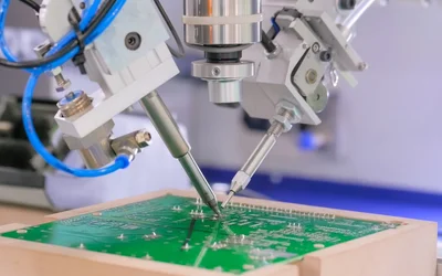
Soldering Unveiled: Exploring Wave and Reflow Techniques for Engineering Graduates. Delve into the Depths of PCB Assembly, Component Compatibility, Production Efficiency, and Quality Assurance. Gain Profound Insights into Wave Soldering Machines, Reflow Ovens, and the Art of Soldering. Empower Your Engineering Journey with this In-Depth Comparative Analysis of Two Key Soldering Methods.
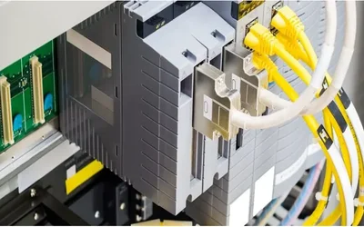
Ladder Logic Programming provides a visual representation of electric circuits for designing and managing automated processes. With its roots in relay control systems, Ladder Logic brings simplicity and clarity to the digital world. Widely used in Programmable Logic Controllers, mastering Ladder Logic is essential for navigating and excelling in the automation-driven industrial landscape.
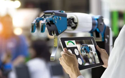
HMI is a dashboard or user interface that play as the communication bridge between humans and systems, machines, or devices. Read on to know the history, characteristics, advantages, and applications of HMI in different industries.

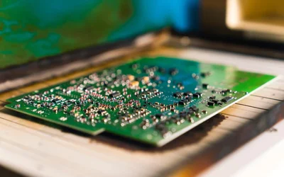
This article provides a detailed overview of the solder reflow process, types of reflow ovens, temperature profiles, solder paste composition and selection, reflow process potential challenges, solutions, inspection, and quality control techniques.
The Creality Ender 3 Pro offers good value for money but lacks an automatic bed leveling feature. Fortunately, Ender 3 Pro bed leveling can be painless with the right tools and preparation.

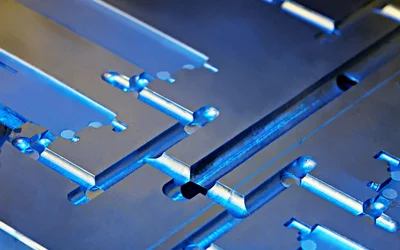
Everything you need to know about metal injection molding (MIM), covering everything from the first step in the process, to materials, applications, and more.

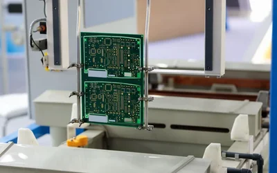
This guide dives deep into the world of PCB surface finishes: In this article, you will experience a comprehensive analysis of various types, factors for optimal performance, and comparing different PCB finishes to choose right one for your specific application
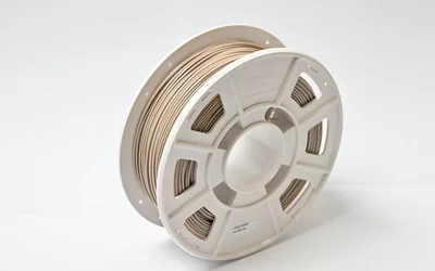
With its ability to produce ultra-robust, temperature-resistant final parts, PEEK 3D printing is becoming the manufacturing process of choice for more and more engineers.
Understanding Plasma Etching: Detailed Insights into Its Techniques, Uses, and Equipment Maintenance
Plasma etching is a salient process in various engineering fields, especially in electronics and materials science. It's a method used to etch or carve fine patterns on the surface of substrates, such as silicon wafers used in semiconductor manufacturing. It works by creating a plasma or ionized gas within a chamber, which chemically reacts with the material on the substrate's surface, effectively removing it. Plasma etching is highly precise and allows for the creation of extremely intricate patterns at a microscopic level.

With its rubber-like material properties, TPU is a versatile 3D printing material that can be used for numerous applications. Here's what you need to know about 3D printing TPU, from filament storage, to printer settings, and more.

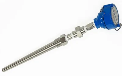
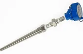
Resistance Temperature Detectors (RTDs) are temperature sensors that vary electrical resistance in response to temperature variations. This page gives a comprehensive introduction of RTDs, including their operation, kinds, uses, benefits, and limits. RTDs are suitable for temperature measurement in sensitive industrial applications due to their high precision, stability, and repeatability. They are utilised in a variety of sectors such as chemical, automotive, aerospace, pharmaceutical, and food & beverage. While they are more expensive than some other temperature sensors, their benefits make them an excellent choice for applications requiring precision and stability.
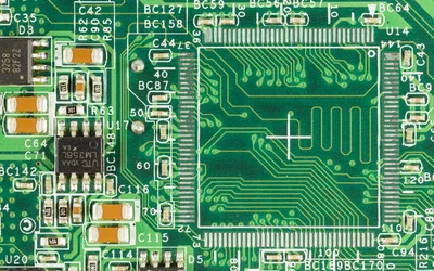
Printed Circuit Boards (PCBs) are an essential component of nearly every electronic device, providing the foundation for the connections and features that enable functionality. As technology advances and devices become more complex, the importance of efficient and effective PCB layout design has become increasingly critical. This article will guide you through designing a PCB layout, from understanding the basics to mastering advanced techniques and preparing for manufacturing.
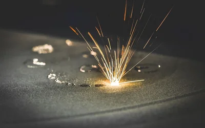
Breaking the Mold: How SLS Printing is Shaping the Future of Manufacturing with Unmatched Precision, Efficiency, and Creative Freedom
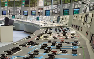
A distributed control system (DCS) is a network of interconnected controllers, computers and other automation devices used to monitor and control production processes. Get an in-depth look into the architecture, components, and applications of distributed control systems.

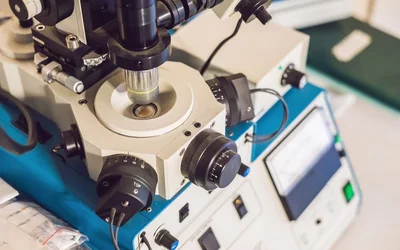
Ion milling is a material etching technique used extensively in modern manufacturing and research. It involves the bombardment of a sample with charged particles, called ions, to remove material from the surface in a controlled manner. This article explores the fundamental principles of ion milling, the various techniques used, the equipment required, and its applications in different fields.

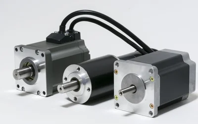
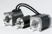
In this article, we will delve into the key factors that differentiate stepper and servo motors, including their operating principles, torque characteristics, control methods, and suitability for different applications.
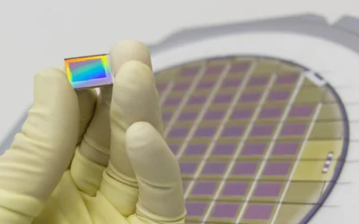
Wafer dicing separates individual integrated circuits or chips from a semiconductor wafer without damaging their delicate structures and circuits. This process is crucial for the production of electronic devices and components used in various industries, and the demand for it has increased with the development of high-performance and smaller electronic devices. Different dicing techniques, such as blade dicing, laser dicing, and plasma dicing, have been developed, and new innovations continue to emerge to address the challenges of complex semiconductor devices.

Learn the powerful approach of combining data from multiple sensors to enhance the overall perception, reliability, and decision-making capabilities of various systems with ease.

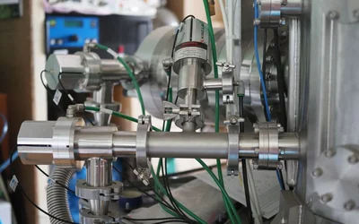
An Overview of Magnetron Sputtering and its Applications in Thin Film Growth

In this article, we will dive deep into the world of simultaneous localization and mapping using Lidar technology. Lidar SLAM has been gaining popularity in recent years, thanks to its versatility and applications across various domains, including autonomous vehicles, mobile robotics, and indoor mapping.

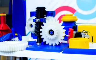
Read on to learn how material choice, print and slicer settings, and post-processing influence the strength of 3D printed parts.