





Article #4 of Power Management for Tomorrow’s Innovations Series: This article investigates the effect that power designs have on the phase noise of Radio Frequency amplifiers through an experiment comparing the performance of three power regulators at different frequencies.
Be the first to know.
Get our electronics weekly email digest.
Tagged with
electronics
ORGANIZATIONS. SHAPING THE INDUSTRY.
Latest Posts

Article #3 of Power Management for Tomorrow’s Innovations Series: Digital Power System Managers facilitate accurate measurement of the output current to let power supplies operate reliably and offer protection in case of electrical faults.

4 ways to improve part design through customisation, material considerations, iterative prototyping with multi-cavity tooling, and the use of digital manufacturing resources

8 minutes read

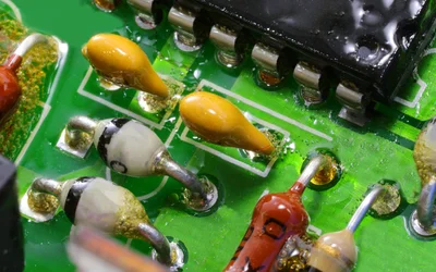
Conformal coating protects from damage caused by fungus, moisture, salt spray, or corrosion.

3 minutes read

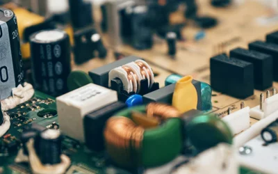
This article explores active filter types, circuit design principles, frequency response, and key differences between active and passive filters.

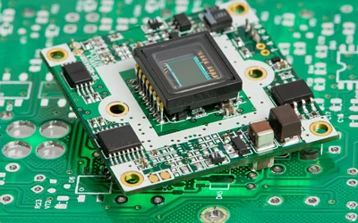
Circuit card assemblies (CCA) give birth to a complete printed circuit board (PCB) after assembling every component. A printed circuit board has no electrical components and needs to go through a manufacturing process called circuit card assemblies which are the complete board assembly.
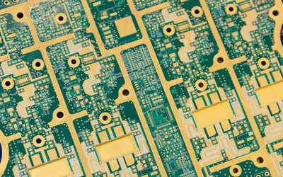
A short primer on how to choose PCBA surface finishes
4 minutes read

Researchers have designed smart, colour-controllable white light devices from quantum dots, tiny semiconductors just a few billionths of a metre in size, which are more efficient and have better colour saturation than standard LEDs, and can dynamically reproduce daylight conditions in a single light

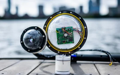
The device could help scientists explore unknown regions of the ocean, track pollution, or monitor the effects of climate change.


The pace of change in consumer electronics has always been fast which poses its own challenges for manufacturers. Here we take a look at 7 trends that will shape the future of product development and manufacturing in the industry…
4 minutes read

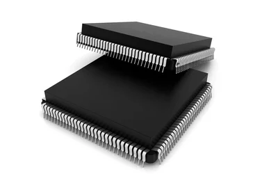
Integrated circuit (IC) package types encompass a range of protective enclosures designed to shield semiconductor components from physical damage and corrosion. This article explores the various classifications of IC packages, each tailored to specific requirements and applications.
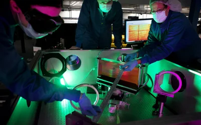
The ZEUS laser at the University of Michigan has begun its commissioning experiments

4 minutes read

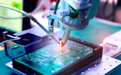
Solder flux has a large impact on final product quality. This article reviews how to use flux during soldering and how to decide on the right technology options for your project.
4 minutes read

Printed Circuit Board Vertical Interconnect Access (PCB VIAs) are small plated holes that create electrical connections between different circuit board layers. This article delves into the various types, functions, and best practices of PCB VIAs to help you optimize your PCB design.
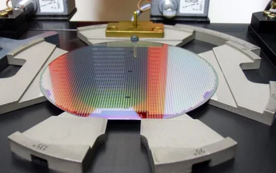
Wafer thinning is a part of the semiconductor manufacturing process. It is essentially grinding off the backside of the wafers to control their thickness and is useful for the production of ultra-thin wafers. These flattened wafers are used to effect stacked and high-density packaging in compact or microelectronic devices. This article discusses the meaning of wafer thinning, along with its various techniques and significance.