


Companies with strong ESG performance reduce costs by 5 to 10 percent.

7 minutes read
Tagged with
Companies with strong ESG performance reduce costs by 5 to 10 percent.
7 minutes read
This 75-page e-book will provide you with the design skills to develop exceptional PCBAs that not only meet but surpass their intended objectives.
4 minutes read
An In-depth Analysis of Features, Applications, and Selection Criteria for Embedded Systems Design. Discover the Advantages and Limitations of SPI, I2C, and UART for Efficient Data Exchange in Various Scenarios.
Mesh topology is the most used network topology, as all computer networks are connected. Each computer sends signals and relays the data from other computer networks. The dedicated link transmits information from one node to another and connects all the nodes.
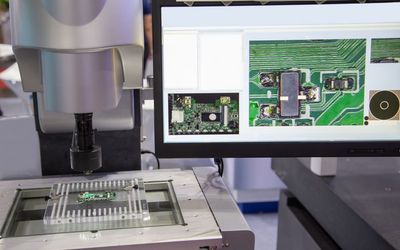
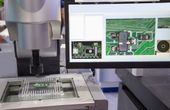
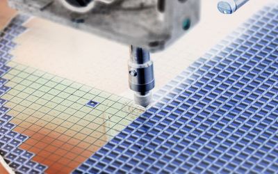
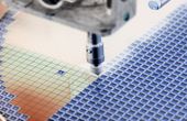
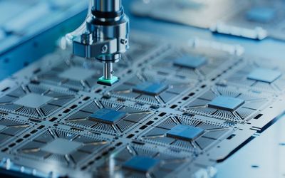
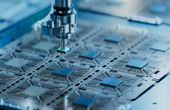
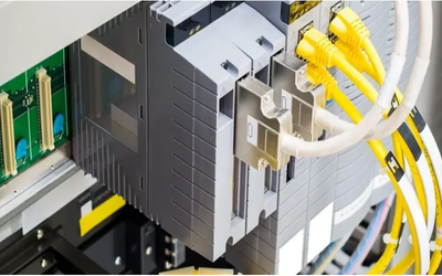
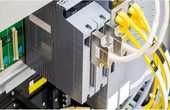
2D and 3D Automated inspection systems are often used for detecting manufacturing errors in fast production lines. Learn how they provide a comprehensive and efficient solution for quality assurance.
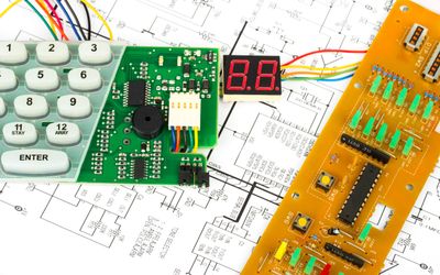
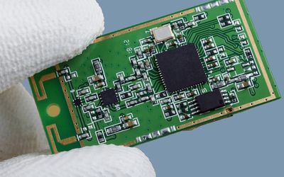
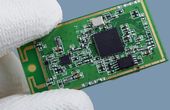
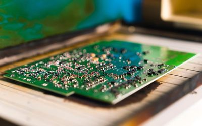
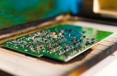
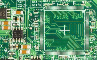
With the increasing need for critical applications technology, PCBAs have become smaller and more complex, requiring designers to create more individual designs in a shorter timeframe. Learn how to do so while avoiding common errors that can derail your project.
8 minutes read
Fifteen percent of electronic parts disappear from the market annually. Are you ready if one of them is part of your design?
5 minutes read
Silicon, with its abundant availability and unique properties, serves as the fundamental building block for semiconductor manufacturing. Its semi-metallic nature makes it an ideal material for controlled conduction of electricity. Furthermore, the combination of silicon with oxygen produces silicon dioxide, a crucial insulating component in silicon chip manufacturing.
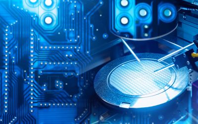
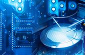
Die attach, also known as die bonding or die mount, is a process used in the semiconductor industry to attach a silicon chip to the die pad of a semiconductor package's support structure, such as a leadframe or metal can header. This article explores the fundamentals of die attach, its importance, materials, and methods used in die attach, its parameters, quality, and reliability techniques.
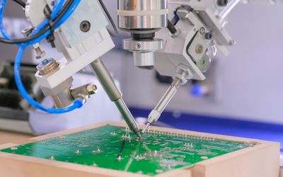
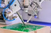
Soldering Unveiled: Exploring Wave and Reflow Techniques for Engineering Graduates. Delve into the Depths of PCB Assembly, Component Compatibility, Production Efficiency, and Quality Assurance. Gain Profound Insights into Wave Soldering Machines, Reflow Ovens, and the Art of Soldering. Empower Your Engineering Journey with this In-Depth Comparative Analysis of Two Key Soldering Methods.
Ladder Logic Programming provides a visual representation of electric circuits for designing and managing automated processes. With its roots in relay control systems, Ladder Logic brings simplicity and clarity to the digital world. Widely used in Programmable Logic Controllers, mastering Ladder Logic is essential for navigating and excelling in the automation-driven industrial landscape.
This article provides a detailed overview of the solder reflow process, types of reflow ovens, temperature profiles, solder paste composition and selection, reflow process potential challenges, solutions, inspection, and quality control techniques.
Surface profile is vital for material performance across industries. A deep understanding of it will help engineers optimize material properties, enhance product performance, and ensure component durability. This article explores its fundamentals, significance, and diverse applications.
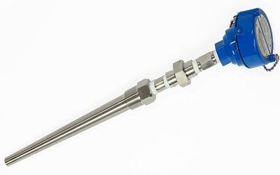
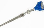
Resistance Temperature Detectors (RTDs) are temperature sensors that vary electrical resistance in response to temperature variations. This page gives a comprehensive introduction of RTDs, including their operation, kinds, uses, benefits, and limits. RTDs are suitable for temperature measurement in sensitive industrial applications due to their high precision, stability, and repeatability. They are utilised in a variety of sectors such as chemical, automotive, aerospace, pharmaceutical, and food & beverage. While they are more expensive than some other temperature sensors, their benefits make them an excellent choice for applications requiring precision and stability.
Printed Circuit Boards (PCBs) are an essential component of nearly every electronic device, providing the foundation for the connections and features that enable functionality. As technology advances and devices become more complex, the importance of efficient and effective PCB layout design has become increasingly critical. This article will guide you through designing a PCB layout, from understanding the basics to mastering advanced techniques and preparing for manufacturing.