


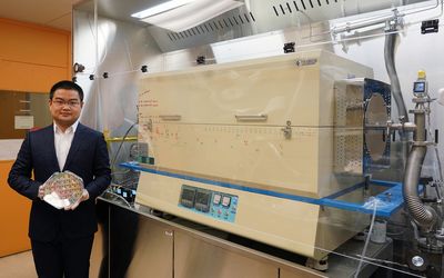
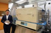
A perovskite-based device that combines aspects of electronics and photonics may open doors to new kinds of computer chips or quantum qubits.
Be the first to know.
Get our electronics weekly email digest.
Tagged with
electronics
ORGANIZATIONS. SHAPING THE INDUSTRY.
Latest Posts
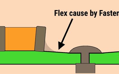
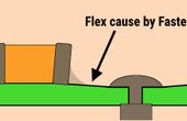
Picking the right fastener can be tricky.

4 minutes read
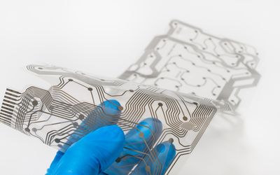
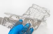
Step into the cutting-edge technologies and future trends of flexible and printed electronics.
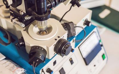
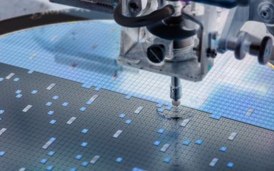
Ion milling is a material etching technique used extensively in modern manufacturing and research. It involves the bombardment of a sample with charged particles, called ions, to remove material from the surface in a controlled manner. This article explores the fundamental principles of ion milling, the various techniques used, the equipment required, and its applications in different fields.
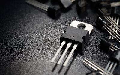
In this article, we will delve into the structure and operation of NMOS and PMOS transistors, and discuss the applications and characteristics of these essential components in electronic circuits.
A new low-temperature growth and fabrication technology allows the integration of 2D materials directly onto a silicon circuit, which could lead to denser and more powerful chips.

In today's interconnected world, network topologies play a crucial role in determining the efficiency and reliability of communication between devices. One such network topology is the bus topology, known for its simplicity and cost-effectiveness. In this comprehensive guide, we will delve deeper into bus topology, exploring its advantages, disadvantages, applications, and the future of this network design.

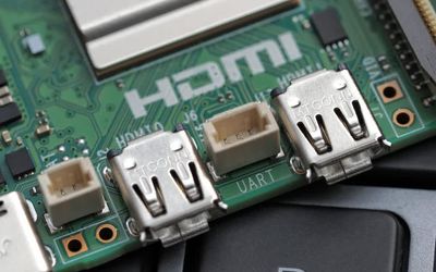
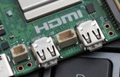
UART and SPI are key communication methods in electronics. UART is ideal for simple, long-distance connections, while SPI excels in fast data transfer. Used in GPS modules, SD cards, and microcontrollers, understanding their differences can help you choose the best for any given project.
Thermal analysis can identify key areas of temperature risk. Learn design strategies for coping with and dissipating excess heat.
2 minutes read
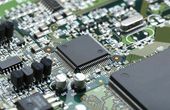
PCB mounting is critical for ensuring the lifetime and dependability of electronic products, including careful component selection and location, adherence to industry standards, and the use of high-quality materials and assembly procedures. This post will go over PCB mounting techniques, tips, and best practices and expand on crucial aspects of printed circuit board mounting.
FPGAs are reprogrammable integrated circuits that enable customizable digital logic designs, providing designers and engineers with a rapid prototyping platform for building complex, efficient, and innovative digital electronic solutions.
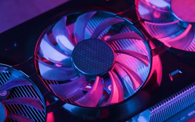
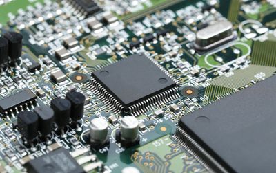
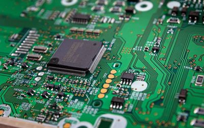
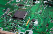
Semiconductors have become an integral part of our modern lives that relies heavily on electronics, serving as the foundation for a wide range of such devices, from smartphones and computers to medical equipment, automotive applications, and renewable energy systems.
The purpose of this article is to provide a comprehensive, in-depth guide to PCB soldermask, exploring the key concepts, principles, and practical applications that will help you excel in PCB design and manufacturing.
New fabs will focus on making cutting-edge chips, not those based on older, established technology. So how should your company solve for potential limited supplies?
4 minutes read

ASIC design is the specialized practice of developing chips tailored to perform specific tasks with maximum efficiency, precision, and reliability—combining architectural insight, hardware expertise, and careful trade-offs to meet exact functional and system-level requirements.