


In the ever-evolving world of processor architectures, the showdown between RISC-V and ARM sparks fervent competition. With their distinct histories, these two giants are redefining computing power and igniting discussions on openness, customization, and innovation in microprocessors.
Be the first to know.
Get our electronics weekly email digest.
Tagged with
electronics
ORGANIZATIONS. SHAPING THE INDUSTRY.
Latest Posts
As electronics become smaller and more powerful, heat dissipation has become a major concern.

8 minutes read

Electronic Technology Supporting the Evolution of “Next Tech”

6 minutes read

Silicon has emerged as the most widely used semiconductor material in the electronic industry, paving the way for the digital age. However, many are still oblivious to the unique properties and characteristics that make silicon ideal for a range of applications. This article explores the fundamentals of semiconductor materials, the properties of silicon that make it a prominent player in the semiconductor industry, and its diverse applications in electronic devices.


Building open communication within internal teams is the first hurdle.
6 minutes read

Fostering a culture of continuous improvement encourages team members to contribute ideas and solutions that lead to better products.
Sensors are ubiquitous in our modern world, playing pivotal roles in numerous sectors. This article delves into their fundamental principles, diverse types, and their significant impact across industries.
Castellation PCB is a type of printed circuit board (PCB) that has a series of small, plated through holes along the edges of the board. These holes are used to create a connection between the board and other components in a circuit. This article delves into the design, manufacturing, and testing processes involved in creating castellation PCBs, providing insights into the key considerations and guidelines that engineers and manufacturers should follow to optimize their designs for performance, reliability, and manufacturability.

Article 3 of Bringing Intelligence to the Edge Series: Balancing the critical metrics of accuracy, power consumption, latency, and memory requirements is key to unlocking the potential of Tiny Machine Learning (TinyML) in low-power microcontrollers and edge computing.

Article 2 of Bringing Intelligence to the Edge Series: Advancements in AI and embedded vision technologies are revolutionizing various industries, enabling real-time decision-making, enhancing security, and facilitating automation in various applications.
Article 1 of Bringing Intelligence to the Edge Series: With the introduction of AI, IoT devices can become more intelligent and less reliant on external systems— but not without trade-offs in performance and cost. Understanding how to make that decision is key.
Introducing the Bringing Intelligence to the Edge Series: Exploring how Artificial Intelligence is moving to embedded systems, transforming technology across various applications.

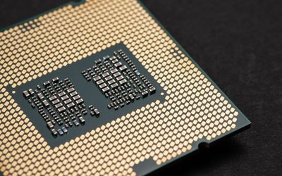
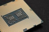
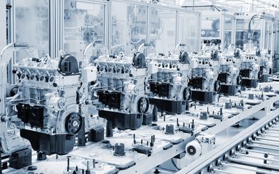
Semiconductors are the building blocks of modern electronics, powering everything from smartphones to satellites. This in-depth guide provides a comprehensive understanding of semiconductors' engineering principles and applications, delving into their fundamental concepts, materials, devices, manufacturing processes, and their impact on today's technology landscape.


The Inflation Reduction Act directs nearly $400 billion to clean energy incentives including $47 billion allocated for manufacturing. This article concentrates on the advantages offered to businesses.
5 minutes read

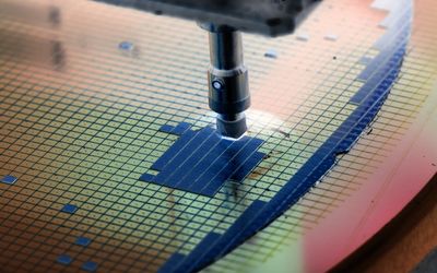
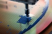
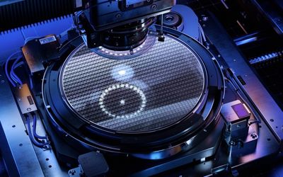
Wafer backgrinding is a crucial step in semiconductor manufacturing, as it prepares the wafer for further processing and packaging. The procedure comprises the thinning of silicon wafers by scraping out material from the backside, which is crucial for enhancing the functionality and dependability of semiconductor devices. This article examines the wafer backgrinding procedure, its difficulties, and the significance of quality control in ensuring the production of high-quality semiconductor devices.