How to Design a PCB Layout: A Comprehensive Guide
Printed Circuit Boards (PCBs) are an essential component of nearly every electronic device, providing the foundation for the connections and features that enable functionality. As technology advances and devices become more complex, the importance of efficient and effective PCB layout design has become increasingly critical. This article will guide you through designing a PCB layout, from understanding the basics to mastering advanced techniques and preparing for manufacturing.

22 May, 2023. 27 minutes read
PCB Design Layout
Introduction
Electronic devices rule our contemporary world. A PCB circuit board is present in all of them, whether they are smartphones with a continuous stream of notifications or widgets that passively monitor vital signs. To meet the rising demands of newer, quicker, and more complicated electronic circuitry, printed circuit board production has kept expanding over time. Recently, there have been discussions on the procedures involved in creating and designing a PCB circuit board. PCB design is a combination of art and science. Some critical ideas in PCB design significantly rely on what you learned in your earlier electronics studies. [1]
However, choosing components, arranging them on a circuit board, and connecting them with copper all demand ingenuity in PCB design. The design of the bare board itself, which serves as the basis for PCB design and production, is another consideration. This article will arm you with the knowledge necessary to begin designing PCBs. Read on to learn more.
Understanding the Basics of PCB Design
What is a PCB?
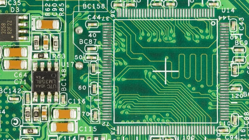
A Printed Circuit Board (PCB) is the backbone of most electronic devices, serving as the platform that hosts electronic components and establishes electrical connections between them. PCBs are made of a non-conductive substrate material, typically fiberglass reinforced with epoxy resin, known as FR4. This substrate is laminated with copper layers, which are etched away to create traces, or conductive pathways, that connect components and enable the flow of electrical signals.
PCBs have revolutionized electronics by providing a compact and efficient means of connecting components, such as resistors, capacitors, and integrated circuits. They have enabled the miniaturization of electronic devices and have facilitated the development of complex and advanced technologies. By understanding the fundamental principles and materials of PCBs, designers can make informed decisions when creating their own PCB layouts.[2]
Types of PCBs
Three main types of PCBs exist. Namely; single-sided, double-sided, and multilayer. Each type has its own unique features and applications, which are crucial for designers to consider when creating a PCB layout.
Single-sided PCBs are the most basic form of printed circuit boards, featuring a single layer of conductive material, usually copper, on one side of the substrate. Components are typically mounted on the non-conductive side, and the conductive side contains the copper traces that electrically connect the components. Single-sided PCBs are cost-effective and suitable for simple electronic devices, such as calculators and sensors.
Double-sided PCBs consist of two layers of conductive material on both sides of the substrate, with components mounted on either side. These PCBs use through-hole technology or surface mount technology to establish electrical connections between the layers. Vias, small holes filled with conductive material, are drilled through the board to connect traces on opposite sides. Double-sided PCBs are more versatile than single-sided boards, allowing for increased component density and more complex circuit designs, such as power supplies and consumer electronics.
Multilayer PCBs have three or more layers of conductive material sandwiched between insulating layers, known as prepreg and core materials. These PCBs use blind and buried vias to connect the internal layers, providing additional routing space for complex circuits. Multilayer PCBs are ideal for high-speed, high-density, and high-power applications, such as computer motherboards, telecommunications equipment, and medical devices. They offer advantages like reduced electromagnetic interference (EMI), improved signal integrity, and increased design flexibility, but come at a higher manufacturing cost.
Understanding the different types of PCBs and their applications helps designers choose the most suitable option for their projects, ensuring the best balance between performance, complexity, and cost.
Recommended reading: PCB Layers: Everything You Need to Know
Essential Components of a PCB Layout
A well-designed PCB layout consists of several key elements that work together to ensure the proper functioning and performance of the electronic device. These essential components include:
Traces: Traces are the conductive pathways that electrically connect components on a PCB. They are made by etching away unwanted copper from the board, leaving behind the desired pattern of conductive pathways. The width and spacing of traces are critical for signal integrity, as they influence resistance, capacitance, and inductance, affecting the performance of high-speed and high-frequency circuits. Designers must consider factors such as current carrying capacity and signal integrity when determining trace width and spacing.
Recommended reading: Trace PCB: A Comprehensive Guide
Pads: Pads are small areas of exposed copper on a PCB where components are soldered. There are two main types of pads: through-hole pads and surface mount pads. Through-hole pads are used for components with leads that pass through the board and are soldered on the opposite side. Surface mount pads are used for surface mount components, which have leads that are soldered directly to the pad on the same side of the board. Designers must ensure that pads are correctly sized and spaced to accommodate the components and facilitate proper soldering.
Vias: Vias are conductive holes in a PCB that connect traces on different layers. They are typically filled with conductive material, such as copper, to establish an electrical connection between layers. There are three types of vias: through-hole vias, which connect the top and bottom layers; blind vias, which connect an outer layer to an inner layer; and buried vias, which connect two or more internal layers. Vias are critical in double-sided and multilayer PCBs, enabling designers to route traces between layers and increase the density of components and connections.[3]
Component footprints: A component footprint is a representation of an electronic component's physical dimensions and contact points on a PCB. It includes the pads for soldering, as well as the outline and any relevant markings to help position and identify the component. Accurate footprints are essential for ensuring that components fit correctly on the board and that the electrical connections are properly established. Designers must carefully verify component footprints against manufacturer specifications to avoid errors in the final PCB layout.
Ground and power planes: Ground and power planes are large areas of copper on a PCB that serves as the common reference points for ground and power connections. These planes help distribute power and ground signals throughout the board, reducing voltage drops, minimizing impedance, and improving signal integrity. They also help shield sensitive signals from electromagnetic interference (EMI) and dissipate heat generated by components. Designers should carefully consider the placement and routing of ground and power planes to optimize the performance of the PCB layout.
Designing a PCB Layout: Step by Step
Designing a PCB layout is a meticulous process that requires careful planning, attention to detail, and adherence to industry standards and guidelines. This section outlines the key steps involved in creating a PCB layout, from defining the requirements to generating the final manufacturing files.
Define the Requirements
Before starting the PCB layout design process, it is crucial to define the requirements and constraints of the project. This involves:
Functionality: Clearly outline the desired functionality of the electronic device, including the specific tasks it must perform, the required inputs and outputs, and any desired user interface elements. This information will guide the selection of components and the overall design of the circuit.
Performance: Identify the key performance criteria for the device, such as speed, power consumption, signal integrity, and thermal performance. These criteria will help determine the necessary design techniques and strategies to achieve the desired performance.
Form factor: Establish the physical dimensions and shape of the PCB, taking into consideration the available space within the enclosure, the orientation of connectors and components, and any required mounting features. The form factor influences the layout of components and traces, as well as the choice of PCB materials and manufacturing techniques.
Cost: Determine the target cost for the PCB, factoring in component costs, manufacturing costs, and assembly costs. The cost constraints can influence the choice of components, the complexity of the design, and the selection of manufacturing processes.
Regulatory compliance: Identify any applicable regulatory standards and requirements, such as safety certifications, electromagnetic compatibility (EMC) standards, and environmental regulations. Compliance with these standards is critical for the successful commercialization of the electronic device and may impact the choice of components and layout techniques.
Defining the requirements and constraints at the beginning of the project ensures a clear understanding of the design objectives and provides a solid foundation for the subsequent steps in the PCB layout design process.[4]
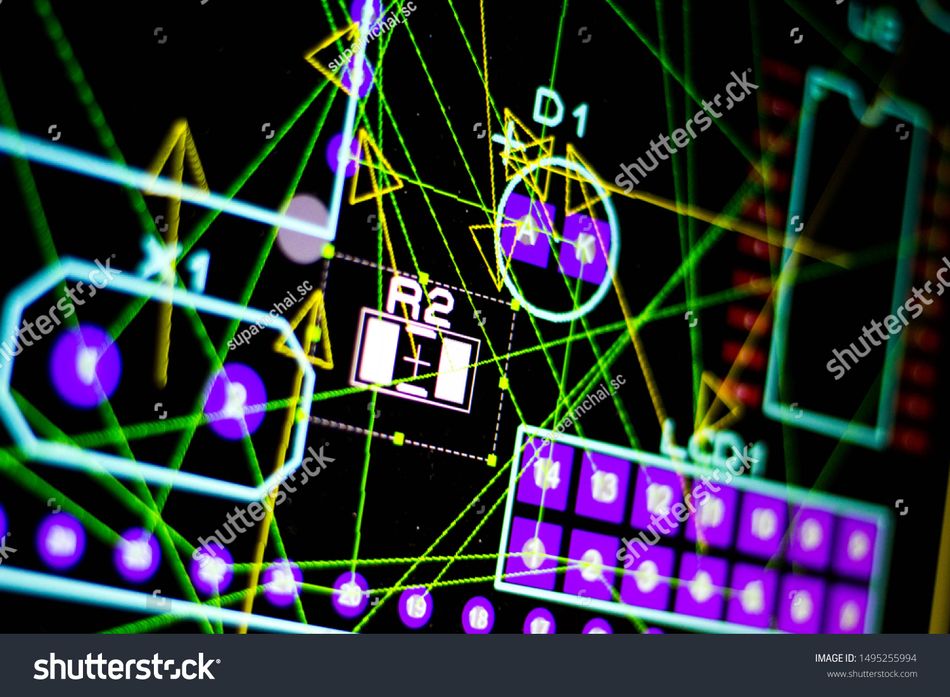
Schematic Design
Given that it serves as the electronic circuit's blueprint, the schematic design phase of the PCB layout is vital. During this phase, a thorough schematic diagram that demonstrates the connections between components and acts as a guide for the physical layout of the PCB is created. Schematic design's essential components include:
Component selection: Choose the appropriate components for the electronic device, considering factors such as functionality, performance, cost, and availability. Components include integrated circuits (ICs), passive components (resistors, capacitors, and inductors), connectors, and other specialized elements such as sensors or actuators.
Circuit design: Design the electrical circuits by connecting the selected components using schematic symbols and wires. This process involves establishing the correct connections between components, defining the required power supply voltages and currents, and ensuring that the circuit meets the desired performance criteria.
Signal integrity: Ensure that the circuit maintains signal integrity by minimizing noise, crosstalk, and signal degradation. This may involve using differential signaling, impedance matching, shielding, or other techniques to reduce interference and maintain signal quality.
Power distribution: Design the power distribution network within the schematic, including power supply connections, voltage regulators, and decoupling capacitors. Proper power distribution is essential for maintaining stable operation, reducing noise, and achieving optimal performance.
Design rules and guidelines: Follow industry-standard design rules and guidelines for the schematic, such as proper component spacing, annotation, and labeling. This ensures that the schematic is readable, well-organized, and can be easily understood by other engineers or PCB layout designers.
Once the schematic design is complete, it is essential to verify its functionality and performance through simulation or analysis. This may include verifying signal integrity, power distribution, and thermal performance. Any issues identified during this stage should be addressed and resolved before moving on to the next step in the PCB layout process, which is the physical layout of the PCB.[5]
Component Placement
The positioning and orientation of each component on the board must be carefully taken into account during the component placement stage of PCB layout creation. This process significantly affects the final product's overall performance, dependability, and manufacturability. The following are the main variables that affect component placement:
Electrical considerations: To minimize signal integrity issues, such as crosstalk and electromagnetic interference (EMI), it is essential to place critical components, like high-speed or sensitive analog components, in close proximity to their respective signal sources or loads. This reduces trace lengths and decreases the potential for signal degradation.
Thermal management: Components that generate heat, like power transistors or voltage regulators, should be positioned in a way that allows for efficient heat dissipation. This may involve placing them near the edges of the board, using thermal vias or heatsinks, or ensuring that there is sufficient airflow around the components.
Mechanical constraints: Account for any physical constraints imposed by the enclosure, mounting points, connectors, or other external factors when placing components on the board. This ensures that the final PCB assembly fits within the designated space and does not cause any mechanical interference.
Assembly and manufacturing: Optimize component placement for ease of assembly and manufacturability by aligning components in a consistent orientation, minimizing the use of components with different package types, and adhering to design-for-manufacturing (DFM) guidelines. This can help reduce manufacturing costs and improve production yield.
Design hierarchy and grouping: Organize components logically based on their functional blocks, such as power supply, microcontroller, or communication interface. This approach makes it easier to route the interconnections between components and reduces the complexity of the layout.
After determining the optimal placement of components on the PCB, it is important to verify that the layout meets all design constraints and requirements. This includes checking for component clearance, adherence to design rules, and ensuring that all electrical, thermal, and mechanical considerations have been addressed. Adjustments to the placement may be necessary based on these verifications to ensure a successful final PCB layout.
Routing
Routing is the process of connecting components on a PCB by creating conductive paths, or traces, between their respective pins. This crucial step ensures that the electrical signals can flow between components as intended, allowing the circuit to function properly. There are several important factors to consider when routing a PCB layout:
Signal integrity: To maintain signal integrity and minimize issues such as crosstalk, reflections, and signal attenuation, it is essential to follow specific routing guidelines. For high-speed digital signals or sensitive analog signals, using controlled impedance traces and keeping trace lengths short is recommended. Additionally, maintaining consistent trace widths and avoiding sharp bends can reduce signal degradation.
Power distribution: To ensure a stable power supply to all components, power traces should be routed with sufficient width and thickness to handle the required current levels. In cases where multiple power supply voltages are needed, separate power planes can be used to provide a low-impedance path for each voltage level. Decoupling capacitors should be placed close to the power pins of ICs to minimize power supply noise.
Grounding: Proper grounding is critical for both signal integrity and electromagnetic compatibility (EMC). A well-designed ground plane provides a low-impedance return path for signals and helps minimize noise and interference. When routing traces, ensure that ground return paths are as short as possible and avoid routing high-speed or noisy signals over ground plane breaks.
Electromagnetic interference (EMI): To minimize EMI, keep high-speed or high-frequency traces away from sensitive components and traces, and avoid running them parallel to each other. Shielding may be necessary in some cases to further protect against EMI. Additionally, maintaining a minimum distance between traces and board edges can help reduce radiated emissions.
Design rules and constraints: Adhere to the design rules and constraints imposed by the PCB fabrication house, which can include minimum trace width, trace spacing, and via sizes. Following these rules ensures that the final PCB can be manufactured without issues.
Routing techniques: Depending on the complexity of the design and the number of layers available, different routing techniques can be employed, such as manual routing, auto-routing, or a combination of both. Manual routing provides more control over the routing process, while auto-routing can save time by automatically generating trace connections based on predefined rules.
After completing the routing process, it is essential to perform design rule checks (DRC) and electrical rule checks (ERC) to verify that the layout meets all design constraints and does not have any issues, such as shorts, opens, or clearance violations. Making any necessary adjustments based on these checks ensures a successful PCB layout design.
Grounding and Power Planes
Grounding and power planes play an essential role in PCB design, providing stable voltage levels and minimizing noise and interference. Designing these planes correctly ensures proper operation and signal integrity of the entire circuit.
Grounding: A ground plane is a large conductive area on the PCB that serves as the common reference point for all components. Proper grounding minimizes noise and electromagnetic interference (EMI) by providing a low-impedance return path for signals. When designing a ground plane, it is essential to create a continuous, uninterrupted surface that covers as much of the PCB as possible. This can be achieved by using a dedicated ground layer or by creating a ground fill on signal layers. It is also important to minimize loop areas by placing components close to their ground connections and avoiding running high-speed or noisy signals over ground plane breaks.
Power planes: A power plane is a large conductive area dedicated to distributing power supply voltages to components on the PCB. The use of power planes reduces voltage drops and impedance, ensuring a stable power supply to all components. In multi-layer PCBs, it is common to have dedicated power planes for different voltage levels, providing a low impedance path for each supply voltage. When designing power planes, minimize the distance between the plane and the components that it powers to reduce power supply noise. Decoupling capacitors should be placed close to the power pins of integrated circuits (ICs) to filter high-frequency noise and maintain voltage stability.
Split and mixed planes: In designs with multiple power supply voltages, split planes can be used to separate the power distribution for different voltage levels. These planes must be carefully designed to avoid creating ground loops or causing interference between voltage domains. Mixed planes can also be utilized, where ground and power planes share the same layer. In this case, proper isolation between the different planes is crucial to avoid cross-contamination of noise between power and ground.
Decoupling: Decoupling is the practice of placing capacitors between power supply pins and ground connections of ICs to minimize voltage fluctuations and high-frequency noise. These capacitors act as local energy storage, providing a stable voltage supply to the IC during transient load changes. When selecting decoupling capacitors, consider factors such as capacitance value, voltage rating, and package size. Additionally, the placement of these capacitors should be as close as possible to the power pins of the ICs, with short, wide traces to minimize inductance.
Proper design and implementation of grounding and power planes in PCB layouts contribute to the overall performance, signal integrity, and electromagnetic compatibility of the circuit. By considering the various factors and guidelines mentioned, designers can ensure a robust and reliable power distribution system within their PCB designs.
Design Rule Check (DRC)
The Design Rule Check (DRC) is a crucial step in the PCB design process, ensuring that the layout adheres to specific manufacturing and performance requirements. This automated process identifies potential issues, such as trace width violations, spacing errors, or missing connections, which could impact the manufacturability and functionality of the final PCB.
Trace width and clearance: One of the key aspects of DRC is verifying that trace widths and clearances meet the manufacturer's specifications. Trace width affects the current-carrying capacity and resistance of the traces, while clearance ensures that there is sufficient space between traces to prevent short circuits or signal interference. DRC checks that the design adheres to these rules, which are often dictated by the fabrication process, materials used, and the expected current levels in the circuit.
Drill hole size and annular ring: The DRC process also verifies that drill hole sizes and annular rings, which are the conductive areas surrounding the holes, meet the manufacturer's requirements. The hole size must be large enough for the intended components or vias, while the annular ring must provide a sufficient area for reliable electrical connections. Inadequate hole size or annular ring dimensions could lead to component fitment issues or poor electrical connections.
Component-to-component spacing: Ensuring proper spacing between components is another critical aspect of DRC. Adequate spacing is necessary to prevent electrical interference, and thermal issues, and facilitate assembly processes like soldering or reflow. DRC checks that component spacing complies with the established rules, which may vary depending on factors such as component size, power levels, or the intended operating environment of the PCB.
Missing connections and unconnected nets: DRC can identify missing connections or unconnected nets within the design, which could lead to functional issues or even failure of the final PCB. By verifying that all components are correctly connected and that all nets have a defined electrical path, DRC helps ensure that the design will function as intended when manufactured.
Silkscreen and solder mask clearance: Another aspect of DRC is checking the silkscreen and solder mask layers for proper clearance and alignment. The silkscreen layer contains component identification and reference designators, which aid in assembly and troubleshooting. The solder mask layer prevents solder bridging and protects the underlying copper from oxidation. DRC ensures that the silkscreen text is legible and does not overlap with pads or vias and that the solder mask openings are aligned correctly with the copper features.
Before going on to the production stage, a comprehensive Design Rule Check is necessary for locating and resolving possible difficulties. The danger of expensive mistakes or revisions can be reduced by designers by sticking to the precise manufacturing and performance criteria, leading to a more effective design process and a higher-quality finished product.[6]
Advanced Techniques in PCB Layout Design
High-Speed Design Considerations
In high-speed PCB design, signal integrity, and electromagnetic compatibility (EMC) become critical factors to ensure reliable performance. Various aspects of the design must be considered to minimize signal degradation and interference.
Transmission lines: At high frequencies, traces on a PCB act as transmission lines, and impedance matching becomes necessary to prevent signal reflections. This can be achieved by designing traces with controlled impedance, which depends on trace width, substrate material, and trace-to-plane separation. Impedance control is essential for maintaining signal integrity and minimizing signal distortion in high-speed applications.
Signal propagation delay: Signal propagation delay is the time taken for a signal to travel from its source to its destination. In high-speed designs, variations in propagation delays can cause timing issues, resulting in signal degradation or data corruption. To mitigate this, designers must carefully route traces of similar lengths for critical signals, often referred to as length matching, to ensure synchronous signal arrival.
Crosstalk: High-speed signals can generate electromagnetic fields that can couple with adjacent traces, causing unwanted interference known as crosstalk. To minimize crosstalk, designers should maintain adequate spacing between parallel traces, avoid routing high-speed signals in parallel for extended lengths, and utilize ground planes as shielding between signal layers.
Differential signaling: Differential signaling is a technique where two complementary signals are transmitted over a pair of conductively coupled traces, reducing the impact of common-mode noise and improving signal quality. In high-speed design, differential pairs are used for critical signals such as USB, HDMI, or Ethernet. To maintain signal integrity, designers must ensure the traces in a differential pair have equal lengths and consistent spacing along their entire route.
Power integrity: Maintaining power integrity is crucial for high-speed designs, as power supply noise can directly impact the performance of sensitive components. Designers should create low-impedance power delivery networks using decoupling capacitors, solid power planes, and well-designed ground planes. Additionally, designers should minimize voltage drops and electromagnetic interference (EMI) by using wide power traces, proper component placement, and careful routing.
By implementing these advanced techniques in high-speed PCB layout design, designers can ensure the reliable performance of their circuits, minimize signal degradation, and achieve optimal electromagnetic compatibility.
EMI and EMC Considerations
Electromagnetic interference (EMI) can adversely affect the performance of a PCB, leading to communication errors, reduced signal integrity, or even system failure. Electromagnetic compatibility (EMC) is the ability of a system to function in the presence of EMI without causing interference to other devices. When designing PCBs, it is crucial to consider EMI and EMC to ensure optimal performance and compliance with regulatory standards.
Partitioning and component placement: To minimize EMI, it is essential to partition the PCB layout according to the function and frequency of components. Grouping similar components together, such as analog and digital parts, reduces the likelihood of interference. Designers should also place sensitive components, such as clock generators or high-speed transceivers, away from potential noise sources like power converters.
Grounding techniques: A well-designed ground plane can significantly reduce EMI by providing a low-impedance path for return currents and shielding sensitive components. Designers should use a continuous ground plane, avoiding slots or cutouts, to minimize loop areas and inductance. In mixed-signal designs, separate analog and digital ground planes can be connected at a single point to prevent interference.
Trace routing: Proper trace routing can help mitigate EMI by minimizing loop areas and reducing the likelihood of crosstalk. High-speed traces should be routed as short and direct as possible, avoiding right angles and parallel runs. Additionally, designers should use multiple layers for signal routing, with ground and power planes placed between them, to reduce electromagnetic emissions.
Power delivery and decoupling: Ensuring a stable power supply is essential for maintaining EMC. Designers should use a solid power plane to provide a low-impedance path for supply currents and minimize voltage drops. Decoupling capacitors should be placed close to components, with values ranging from picofarads to microfarads, to suppress high-frequency noise and maintain power integrity.
Shielding and filtering: In some cases, shielding enclosures may be necessary to protect sensitive components from external EMI or to prevent radiation from high-frequency devices. Designers can use metallic enclosures or conductive coatings to achieve this. Additionally, incorporating filtering components, such as ferrite beads or common-mode chokes, can help reduce EMI by attenuating high-frequency noise.
By considering EMI and EMC in the PCB layout design, designers can ensure that their products perform reliably, meet regulatory requirements, and do not cause interference with other electronic devices.
Thermal Management
Effective thermal management is crucial for maintaining the reliability and performance of electronic devices. Excessive heat can lead to component failure, reduced lifespan, and degraded performance. Therefore, it is essential to consider thermal management strategies when designing PCB layouts.
Component selection and placement: The choice of components can significantly impact the thermal performance of a PCB. Designers should opt for components with lower power consumption and higher thermal efficiency. Additionally, placing heat-generating components, such as power converters or high-current ICs, away from temperature-sensitive components can help prevent hotspots and facilitate heat dissipation.
Thermal vias and copper planes: Thermal vias are small holes filled with conductive material that connect different layers of a PCB to facilitate heat transfer. Designers can place thermal vias beneath or around heat-generating components to improve heat dissipation. Copper planes can also be used as heat spreaders, distributing heat evenly across the PCB and reducing hotspots. The thickness of the copper plane impacts its thermal conductivity, with thicker planes offering better heat dissipation.
Heat sinks and cooling solutions: Attaching heat sinks to high-power components can help dissipate heat by increasing the surface area available for convection. Materials with high thermal conductivity, such as aluminum or copper, are commonly used for heat sinks. In cases where passive cooling solutions are insufficient, active cooling methods, like fans or liquid cooling systems, can be implemented to maintain optimal operating temperatures.
Thermal simulation and testing: Analyzing the thermal performance of a PCB layout through simulation can help identify potential issues before fabrication. Designers can use specialized software to model the heat generation and dissipation of components, allowing them to optimize the layout for better thermal management. After fabricating the PCB, thermal testing using infrared cameras or thermocouples can validate the effectiveness of the implemented thermal management strategies.
Incorporating effective thermal management strategies in PCB layout design helps ensure the reliability and performance of electronic devices, preventing component failure and extending their lifespan.
Software Tools for PCB Layout Design
Designing PCB layouts involves a combination of skills, knowledge, and tools. A variety of software tools are available to facilitate the process, from schematic capture to final output files for manufacturing. These tools help designers achieve optimal performance, adhere to design rules, and streamline the overall process.
Popular PCB Design Software
Altium Designer: Altium Designer is a widely used, comprehensive PCB design software that offers a unified environment for schematic capture, PCB layout, and design documentation. It provides advanced routing capabilities, real-time design rule checking, and integration with mechanical CAD software. Altium Designer supports multi-board and rigid-flex designs, catering to a broad range of applications.
Cadence Allegro: Allegro, developed by Cadence Design Systems, is a popular, feature-rich PCB design software that allows designers to address complex design challenges. With support for high-speed, high-density, and multi-layer designs, Allegro provides advanced signal and power integrity analysis tools, concurrent team design capabilities, and a constraint-driven design process.
Mentor Graphics PADS: PADS, by Mentor Graphics, is a robust PCB design suite aimed at small and medium-sized businesses. It offers an intuitive interface, comprehensive design rule checking, and advanced routing features. PADS integrates with other Mentor Graphics tools, such as HyperLynx for signal integrity analysis, and provides a scalable solution for growing businesses.
Autodesk EAGLE: EAGLE, now owned by Autodesk, is a popular choice for hobbyists, startups, and small design teams. With a user-friendly interface and a comprehensive component library, EAGLE provides an affordable solution for schematic capture and PCB layout design. It supports up to 16 layers and includes basic routing and design rule-checking features.
KiCad EDA: KiCad is an open-source PCB design software that offers a comprehensive suite of tools, including schematic capture, layout, and 3D visualization. It supports multi-layer designs, provides an extensive component library, and offers advanced routing features. As an open-source project, KiCad benefits from a large, active community of contributors and users.
Selecting the right PCB design software depends on factors such as the complexity of the design, budget, and specific feature requirements. Each tool has its strengths and weaknesses, making it essential to evaluate and choose the one that best aligns with the designer's needs and project goals.[7]
Integrating Simulation Tools
Simulation tools play a critical role in PCB design by providing designers with the ability to analyze and optimize their designs before manufacturing. By integrating simulation tools into the PCB design process, designers can identify and address potential issues early on, saving time and reducing the likelihood of costly revisions.
Signal Integrity (SI) Analysis: SI analysis is essential for high-speed digital designs, where signal degradation due to factors such as impedance mismatch, crosstalk, and reflections can lead to data corruption and system failures. SI tools simulate the transmission line behavior of PCB traces and enable designers to identify and correct impedance mismatches, minimize reflections, and optimize the routing of high-speed signals.
Power Integrity (PI) Analysis: PI analysis focuses on maintaining a stable and clean power distribution network (PDN) within the PCB. PI tools simulate voltage drops, noise, and transient responses in the PDN, allowing designers to optimize power planes, decoupling capacitor placement, and power component selection to ensure adequate voltage levels and minimize noise throughout the design.
Electromagnetic Compatibility (EMC) Analysis: EMC tools help designers predict and mitigate electromagnetic interference (EMI) issues that can lead to signal integrity problems, device malfunctions, and non-compliance with regulatory standards. By simulating the radiation and susceptibility of PCB components and traces, designers can optimize board layout, component placement, and shielding strategies to minimize EMI risks.
Thermal Analysis: Thermal analysis tools simulate the temperature distribution across the PCB, helping designers identify potential hotspots and optimize the thermal performance of their designs. By analyzing factors such as component power dissipation, thermal vias, and heat sinks, designers can improve heat dissipation and ensure the reliability and longevity of the PCB.
3D Field Solver: A 3D field solver is an advanced simulation tool that provides a comprehensive analysis of the electromagnetic fields within a PCB layout. This tool can help designers optimize complex designs, such as RF and microwave circuits, by accurately modeling the interactions between components, traces, and dielectric materials.
By integrating simulation tools into the PCB design process, one may speed up development and cut expenses while also improving the quality and performance of the finished product. Designers can reduce the possibility of expensive board changes and enable a more seamless transition from design to manufacture by spotting and fixing any faults early on.
Preparing for PCB Manufacturing
Generating Gerber
When preparing for PCB manufacturing, generating Gerber files is an essential step. Gerber files are the industry-standard format for conveying design information to PCB manufacturers. These files contain the necessary data for fabricating the PCB, such as copper layer patterns, drill holes, solder mask, and silkscreen information.
Gerber files are generated from the design software once the PCB layout is complete and has passed the Design Rule Check (DRC) and Electrical Rule Check (ERC). When generating Gerber files, it is crucial to adhere to the manufacturer's specifications to avoid issues during the fabrication process. Common parameters to consider include the format (RS-274X or X2), units (inches or millimeters), and coordinate precision (e.g., 2:4 or 2:5).
Once the Gerber files are generated, designers should perform a visual inspection using a Gerber viewer to ensure the design's accuracy and quality. This step allows the designer to identify and correct any errors or discrepancies before sending the files to the manufacturer.
In addition to Gerber files, other files may be required for PCB manufacturing, such as:
Drill Files: Drill files provide information on the size and location of holes in the PCB, including through-holes and vias. These files are typically generated in the Excellon format and should be included alongside the Gerber files when submitting the design for manufacturing.
Fabrication Drawing: A fabrication drawing provides a detailed overview of the PCB layout, including dimensions, tolerances, and any special instructions for the manufacturer. This drawing serves as a reference for the fabrication process and should include information such as layer stack-up, hole sizes, and material specifications.
Assembly Drawing: An assembly drawing shows the placement of components on the PCB and is used as a reference during the assembly process. It typically includes a bill of materials (BOM) that lists each component's designator, manufacturer part number, and quantity.
By generating Gerber files and other necessary documentation, designers can ensure a smooth transition from design to manufacturing, reducing the risk of errors and delays in the fabrication process.[8]
Creating a Bill of Materials (BOM)
A Bill of Materials (BOM) is a comprehensive list of components, parts, and materials required to manufacture a printed circuit board. It is a crucial document for the procurement and assembly of the PCB, as it ensures that all necessary components are accounted for and their specifications are clearly defined.
The BOM typically includes the following information for each component:
Designator: A unique identifier that corresponds to the component's reference designator on the PCB layout and schematic.
Manufacturer Part Number (MPN): The specific part number assigned by the component manufacturer. This number is essential for component procurement, as it defines the exact specifications and ensures that the correct parts are ordered.
Description: A brief description of the component, including its function and any relevant specifications.
Quantity: The number of units of the component required for a single PCB.
Package: The physical package or footprint of the component, such as through-hole, surface-mount, or chip-scale package.
Value: The electrical value of the component, such as resistance, capacitance, or inductance.
Tolerance: The acceptable variation in the component's value, usually expressed as a percentage.
Creating an accurate and well-organized BOM is essential for ensuring a smooth PCB manufacturing process. It helps to streamline the procurement of components, reduces the likelihood of errors in assembly, and serves as a reference for future revisions or production runs. [9]
Several best practices can be employed when creating a BOM:
Component consolidation: By using a limited number of unique components and minimizing the number of different values or specifications, designers can simplify the procurement process, reduce costs, and improve assembly efficiency.
Verify component availability: Check the availability of components in the market to avoid delays in production due to long lead times or obsolescence.
Include alternative components: Specify alternative components with similar specifications to ensure that the production process can continue in case of unavailability or obsolescence of the primary component.
Organize the BOM: Organize the BOM in a clear and logical manner, such as grouping components by type or function, to facilitate component procurement and assembly.
Revision control: Implement a system for tracking revisions to the BOM, ensuring that all changes are documented and that the most current version of the BOM is always used in production.
By adhering to these best practices, designers can create a comprehensive and accurate BOM that facilitates a seamless transition from design to manufacturing, ensuring that the final PCB meets the intended specifications and functions as designed.
Selecting a PCB Manufacturer
Selecting the right PCB manufacturer is crucial for ensuring that the final product meets the required specifications and is delivered on time and within budget. Several factors should be considered when choosing a PCB manufacturer to ensure that they can meet the specific requirements of a particular project.
Capabilities: Evaluate the manufacturer's capabilities, including the range of materials they work with, their ability to handle various board sizes and complexities, and their capacity for producing multilayer boards. It is essential to ensure that the manufacturer can meet the technical requirements of the project, such as minimum trace width and spacing, drilling precision, and surface finish quality.
Lead time: Assess the manufacturer's lead times for both prototype and production runs. Faster lead times can be critical for meeting project deadlines and enabling iterative design improvements. However, it is important to balance lead time against quality, as some manufacturers may sacrifice quality to meet aggressive schedules.
Quality certifications: Look for manufacturers with relevant industry certifications, such as ISO 9001 and IPC standards, which demonstrate their commitment to quality management and adherence to industry best practices.
Experience: Consider the manufacturer's experience in producing PCBs for similar applications or industries. An experienced manufacturer is more likely to understand the unique challenges and requirements of a specific project and can often offer valuable insights and suggestions for optimizing the design for manufacturability.
Cost: Compare the costs of different manufacturers, taking into account factors such as tooling and setup fees, per-unit costs, and any additional charges for shipping or handling. It is essential to find a balance between cost and quality, as the cheapest option may not always provide the best results.
Customer service and communication: Evaluate the manufacturer's responsiveness and communication, as these factors can significantly impact the success of a project. A manufacturer that is easy to communicate with and provides timely updates can help avoid misunderstandings and ensure that any issues are resolved quickly.
Location: Consider the manufacturer's location, as this can affect shipping times and costs, as well as the ease of communication due to time zone differences. While offshore manufacturers may offer lower costs, working with a local manufacturer may provide advantages in terms of faster shipping and more effective communication.
By carefully considering these factors and conducting thorough research, designers can select a PCB manufacturer that meets the specific requirements of their project, ensuring that the final product is delivered on time, within budget, and to the required specifications.[10]
Conclusion
PCB layout design is a crucial step in the process of electronics manufacturing. A well-designed PCB layout can ensure the proper functioning of the circuit and minimize the risk of errors or failures during production. In this article, we have discussed various aspects of PCB layout design, including its basics, techniques, and tools.
In conclusion, PCB layout design is a critical process that requires careful consideration of various factors, including design rules, layer stack-up, component placement, and manufacturing and testing considerations. By following these guidelines and using the right tools, engineers can design high-quality PCB layouts that meet the requirements of their applications.
Frequently Asked Questions (FAQs)
1. What is the importance of stack-up in PCB design?
Stack-up is a critical aspect of PCB design, as it defines the arrangement and thickness of the layers in a multilayer board. A well-designed stack-up can help minimize signal integrity issues, reduce electromagnetic interference (EMI), and optimize the board's mechanical and thermal properties. It is essential to consider factors such as impedance control, EMI shielding, and thermal management when defining the stack-up.
2. How can designers mitigate EMI and EMC issues in PCB layout?
To minimize EMI and EMC issues, designers should follow best practices, such as grounding techniques, proper component placement, minimizing loop areas, and maintaining sufficient clearance between high-speed signals and other traces. Additionally, incorporating filtering and shielding techniques, as well as using differential signaling for high-speed signals, can further help reduce EMI and ensure compliance with EMC regulations.
3. Why is thermal management important in PCB design?
Thermal management is crucial for maintaining the reliability and performance of electronic components. Excessive heat can lead to premature component failure, signal integrity issues, and reduced operating life. Designers must consider factors such as component placement, thermal vias, and heat sinks to ensure efficient heat dissipation and maintain the board and components within their specified operating temperature ranges.
4. What are some popular PCB design software tools?
Popular PCB design software tools include Altium Designer, Cadence OrCAD, Autodesk EAGLE, and KiCad. These software packages offer various features and capabilities for schematic capture, PCB layout, and design rule checking, allowing designers to create and optimize their designs efficiently.
5. How do Gerber files and Bill of Materials (BOM) aid in PCB manufacturing?
Gerber files are the industry-standard file format for PCB manufacturing, containing detailed information about the board's layers, copper traces, drill holes, and other features. These files are used by the manufacturer to create the physical PCB. A Bill of Materials (BOM) lists all the components required for the PCB assembly, including their reference designators, part numbers, and quantities. The BOM is crucial for the manufacturer to source and place the correct components on the board during assembly.
References
WellerPCB, 2023. Al Technology-Electronic Design and Manufacturing. [Cited 2023 May 12]. Available from: https://wellerpcb.com/al-technology-electronic-design-and-manufacturing/
PCBCart, 2022. Printed Circuit Board Introduction & PCB Types. [Cited 2023 May 12]. Available from: https://www.pcbcart.com/article/content/PCB-introduction.html
Abiola Ayodele (Wevolver), 2022. Trace PCB: A comprehensive Guide. [Cited 2023 May 12]. Available from: https://www.wevolver.com/article/trace-pcb-a-comprehensive-guide
Millenium Circuits Limited, 2023. PCB Layout Consideration. [Cited 2023 May 13]. Available from: https://www.mclpcb.com/blog/pcb-layout-considerations/
Electronics Technology, n/a. Printed Circuit Board Design. [Cited 2023 May 13]. Available at: https://www.vpitechnology.com/product-design-and-development/pcb-design#:~:text=A%20PCB%20design%20schematic%20can,design%20layout%20of%20the%20circuit.
Sierra Circuits, 2021. Design Rule Check (DRC) for PCB Manufacturing. [Cited 2023 May 13]. Available at: https://www.protoexpress.com/blog/drc-pcb-manufacturing/#:~:text=What%20is%20design%20rule%20check,the%20products%20that%20are%20manufactured.
G2, 2023. Best PCB Design Software. [Cited 2023 May 14]. Available at: https://www.g2.com/categories/pcb-design
WELL PCB. PCB Fabrication Process - 20 Steps Ultimate Guide on PCB Manufacturing. 2022. [Cited 2023 Jan 3] Available from: https://www.wellpcb.com/pcb-fabrication-process.html
PCBCart, 2022. How to Create a BOM (Bill of Materials). [Cited 2023 May 12]. Available from: https://www.pcbcart.com/article/content/creating-a-bom.html
EMSG, 2022. How to Choose a PCB Assembly Company (7-Step process). [Cited 2023 May 14]. Available from: https://emsginc.com/resources/how-to-choose-a-pcb-assembly-company/