Understanding Surface Profile in PCB and Semiconductor Manufacturing
Surface profile is vital for material performance across industries. A deep understanding of it will help engineers optimize material properties, enhance product performance, and ensure component durability. This article explores its fundamentals, significance, and diverse applications.

Last updated on 13 Mar, 2025. 21 minutes read
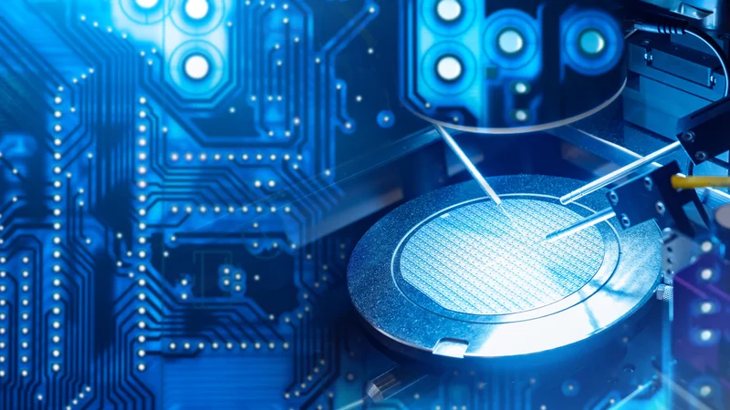
Precision Soldering for Optimal PCB Surface Profile
Introduction
As a key element in engineering and manufacturing, the surface profile represents a material’s texture, topography, or roughness in three dimensions. It is crucial in industries such as automotive, aerospace, electronics, and industrial manufacturing, as it helps optimize performance by quantifying surface characteristics like roughness and irregularities. With parameters such as average roughness (Ra) and peak-to-valley height (Rz), engineers can measure and refine surface properties to enhance friction, wear, adhesion, corrosion resistance, and thermal management, thereby improving material reliability and product durability.
In engineering drawings, the surface profile is controlled through GD&T (geometric dimensioning and tolerancing), a system that defines acceptable deviations in shape and geometry. This is particularly useful for complex or curved surfaces where traditional tolerances like flatness or circularity fall short. Profile tolerances ensure the entire surface adheres to design specifications, not just individual sections, with tools like the CMM (coordinate measuring machine) used to ensure that 3D scans match the CAD model.
Understanding the profile of a surface is critical for optimizing dimensional tolerance and product performance. Unlike the profile of a line, which applies to a single cross-section, the profile of a surface encompasses the entire geometry. Properly applying GD&T symbols, such as those defined in ASME Y14 and ISO standards, helps manufacturers maintain parallelism, perpendicularity, and form control in production. When working with no datums or using a datum feature as a reference, designers must carefully specify the feature control frame and basic dimensions to ensure consistency. These principles are vital for industries requiring high precision, such as aerospace components, medical implants, and high-performance automotive parts.
Recommended reading: What is GD&T: Basics and Definitions
What Is Surface Profile?
Surface profile is the three-dimensional geometry of a material’s surface, capturing its true profile within a specified profile tolerance zone. This includes microscopic and macroscopic contours, textures, and irregularities, significantly impacting performance in electronics, automotive, aerospace, and precision manufacturing.
In electronics, surface profile is critical for components like copper traces on PCBs and doped silicon in semiconductor wafers, where bilateral tolerances ensure uniformity in both positive and negative directions relative to a datum. Key parameters such as average roughness (Ra), peak-to-valley height (Rz), and straightness deviations help quantify surface characteristics. By applying modifiers to tolerance zones, engineers can refine manufacturing constraints, ensuring surfaces remain within controlled limits for optimal electrical conductivity, adhesion, and mechanical integrity.
Theoretical Foundations of Surface Profile
To understand why the surface profile plays a critical role in the performance of electronic devices, it's important to delve deeper into the theories behind surface roughness and texture. These factors are often described and quantified using both statistical and geometric approaches, providing insights into the surface's behavior in various applications, especially in electronics manufacturing.
1. Statistical Parameters for Surface Profile
Surface roughness is commonly quantified using several statistical parameters, each offering a different perspective on the surface's characteristics:
Ra (Arithmetic Mean Roughness): Ra is one of the most frequently used parameters for surface roughness. It measures the average deviation of the surface heights from the mean line over a given sampling length. This value provides a quick assessment of the overall roughness, with smaller Ra values indicating smoother surfaces. For example, in PCB manufacturing, if Ra is too high, it could result in higher friction or poor adhesive bonding during the lamination process.
Rz (Mean Peak-to-Valley Height): This parameter looks at the vertical distance between the highest peak and the lowest valley within a sample. Rz is calculated by averaging the distances of the five highest peaks and the five lowest valleys in the profile. Rz is particularly useful when assessing surfaces with deep grooves or uneven topography. For instance, in semiconductor manufacturing, controlling Rz ensures that the surface of the wafer does not introduce defects during processes like lithography or etching, which could cause electrical failures.
Rq (Root Mean Square Roughness): Rq calculates the square root of the average of the squared deviations from the mean line. Unlike Ra, Rq gives more weight to large deviations, making it more sensitive to outliers. In high-precision applications, such as microelectronics, small variations in surface roughness can lead to significant performance issues, and Rq can help detect those subtle inconsistencies. For example, excessive surface roughness in the active regions of semiconductor wafers can lead to inconsistent electrical characteristics, affecting device performance.
These statistical parameters are derived from sampling data points across the surface, and modern surface metrology systems are capable of generating 2D profiles or even 3D topographical maps. These advanced measurements provide engineers with deeper insights into the surface texture, enabling them to assess how various surface features may impact performance.
2. Surface Topography vs. Surface Roughness
It’s essential to distinguish between surface topography and surface roughness, as they are often used interchangeably but describe different characteristics. Surface topography refers to the complete set of surface features across multiple scales, including larger geometric deviations such as flatness, waviness, and cylindricity. In contrast, surface roughness focuses on smaller-scale irregularities, often at the micrometer or nanometer level, which are superimposed on the broader surface form.
In PCB design, surface roughness directly influences signal integrity, particularly at high frequencies. The outer copper layer may exhibit an inherent treatment pattern, impacting electrical conductivity. If the roughness exceeds the allowable profile tolerance zone, signal losses can occur, especially for high-speed signals. Meanwhile, surface topography plays a broader role in mechanical fit and assembly alignment within the datum reference frame.
For semiconductor wafers, precise control of surface topography is critical, as wafer flatness affects key manufacturing processes such as photolithography and wafer bonding. Even minimal topographical deviations can lead to defects in pattern transfer or layer adhesion. Angularity and datum references, such as Datum A, ensure proper alignment in these high-precision applications. Additionally, applying material condition modifiers allows for controlled variations in surface geometry, optimizing manufacturing tolerances while maintaining functional performance.
Recommended reading: Silicon Wafers: Production, Properties and Application
3. Impact on Electronics
The surface profile has profound implications for the performance and reliability of electronic devices. Several key areas are directly influenced by the surface texture:
Conduction Losses: High-frequency signals traveling along the traces of a PCB experience losses due to the skin effect, where the current tends to flow on the outer surface of conductors. Surface roughness exacerbates this effect, leading to higher resistance and, consequently, signal attenuation. For example, in high-speed PCBs used for RF (radio-frequency) applications, excessive surface roughness can degrade the signal integrity, making it harder to maintain data transmission quality.
Dielectric Interface: In multi-layer PCBs, the interface between copper layers and dielectric materials plays a critical role in ensuring signal integrity. If the surface of the copper is too rough, it can cause localized air gaps or irregularities, leading to changes in impedance. This can create problems such as signal reflection or crosstalk, particularly at higher frequencies. In designs that require precise impedance control, such as high-performance communication devices, it is essential to maintain a smooth and consistent surface profile throughout the manufacturing process.
Wafer Processing: Surface profile control is also vital in semiconductor manufacturing. In processes such as wafer bonding or lithography, uniformity in the surface profile ensures better pattern definition and precise alignment. Any irregularities on the surface can result in the misalignment of photomasks, leading to defects in the final wafer. For example, if the wafer's surface has excessive roughness or waviness, it can interfere with the deposition of thin films or the etching process, compromising the electrical characteristics of the chips.
Recommended reading: Chips and Wafers: What's the Difference?
Surface Profile in PCB Manufacturing
The surface profile plays a significant role in PCB (Printed Circuit Board) manufacturing, influencing everything from adhesion to performance in high-speed applications. By carefully controlling the roughness of materials like copper foil and surface finishes, manufacturers ensure the integrity and reliability of the final product.
1. Copper Foil Roughness
The roughness of the copper foil used in PCB manufacturing is an essential factor in determining the quality of the board's electrical performance and adhesion. PCB manufacturers typically purchase copper foil with a specified roughness, which can either enhance or hinder the overall performance of the board. While a rougher surface is beneficial for ensuring good adhesion to dielectric materials, it can become a liability for high-speed designs, where signal integrity is paramount.
To address this issue, LoRa (low roughness) copper foils have become increasingly popular, particularly for RF (Radio Frequency) and microwave applications. These foils reduce insertion losses by offering smoother surfaces, which are crucial for high-frequency signals.
Common Copper Foil Types and Their Applications
Foil Type | Roughness (Typical Ra) | Applications |
Standard ED (Electrodeposited) | 3.0 - 4.5 µm | General-purpose PCB fabrication |
Rolled Annealed (RA) | 1.0 - 2.0 µm | Flexible circuits, high-frequency applications |
Very Low Profile (VLP) | ≤ 0.5 - 1.0 µm | High-speed digital, RF, and microwave designs |
Electrodeposited Copper (ED): This type of copper is made by depositing copper onto a rotating drum. It typically results in a matte side (rougher) and a drum side (smoother). The roughness of the matte side can help in adhesion to dielectrics, but for high-speed circuits, the rougher surface could lead to signal losses and increased insertion loss.
Rolled Annealed Copper (RA): This copper is created by mechanically rolling the material, which results in a smoother surface. It is particularly suited for applications requiring flexibility and lower frequencies as it offers better performance in these areas.
Very Low Profile Copper (VLP): VLP copper undergoes special treatments to minimize roughness, making it ideal for high-speed and high-frequency applications. In RF and microwave designs, the reduced surface roughness allows for improved signal transmission with fewer losses, which is vital in high-performance electronics.
2. Surface Finishes for PCBs
Besides copper foil, the choice of surface finish plays a significant role in the final surface profile of a PCB. Surface finishes such as ENIG (Electroless Nickel Immersion Gold), HASL (Hot Air Solder Leveling), and OSP (Organic Solderability Preservative) are commonly used to enhance solderability and provide protective coatings. Each finish affects the surface roughness differently and is chosen based on the specific needs of the PCB’s application.
ENIG (Electroless Nickel Immersion Gold): ENIG is widely regarded for its smooth surface and corrosion resistance, making it ideal for fine-pitch components. The smooth finish ensures good solderability and minimizes the risk of solder bridging during assembly, particularly for surface-mount components that require precision.
HASL (Hot Air Solder Leveling): This finish involves dipping the PCB in molten solder and using hot air to level the surface. While it offers a reliable, cost-effective solution, it can result in uneven surfaces due to the nature of the hot solder leveling process. This unevenness can be problematic in high-frequency applications, where a smooth surface is crucial for consistent signal transmission.
OSP (Organic Solderability Preservative): OSP is a thin organic layer that preserves the solderability of copper surfaces without significantly altering roughness. It is often used in combination with other finishes for added protection. OSP is particularly useful for designs that don't require the level of durability or smoothness that other finishes, like ENIG, provide.
Recommended reading: HASL vs ENIG: Choosing the Right PCB Surface Finish
3. IPC-6012 Standards
The IPC-6012 standard, established by the Institute for Printed Circuits (IPC), sets guidelines for the quality and manufacturing of PCBs, including acceptable levels of surface irregularities. While it does not specify an exact maximum roughness for each layer, the standard provides pass/fail criteria for parameters such as plating thickness, conductor surface uniformity, and overall workmanship. This ensures that PCBs meet the functional requirements for general applications.
However, in high-speed designs—such as those used in 5G communications, automotive radar systems, and satellite technology—engineers often go beyond these standards. They collaborate with PCB fabricators to specify precise roughness targets for each layer. In these advanced applications, even slight deviations in surface profile can lead to significant performance degradation, making it essential to control surface roughness to strict specifications.
For example, in 5G technology, where signal integrity is crucial, a smooth surface is necessary to minimize signal losses and ensure efficient data transmission. The use of Very Low Profile (VLP) copper and precise surface finishes such as ENIG can significantly improve the performance of 5G devices, where high-frequency signals must be transmitted with minimal attenuation.
Surface Profile in Semiconductor Manufacturing
In semiconductor manufacturing, surface profile control is even more critical than in PCB production, as the demand for sub-nanometer flatness and precise topographies is essential for ensuring the performance of integrated circuits. Unlike PCBs, which focus on copper roughness, semiconductor wafers must meet incredibly stringent flatness requirements to ensure proper functioning in advanced technologies.
1. Wafer Flatness and Roughness
In semiconductor wafer manufacturing, the surface profile is crucial to the performance and yield of the chips. Two important parameters to consider are Total Thickness Variation (TTV) and surface roughness on active layers, which are tightly controlled to meet the demands of smaller process nodes.
TTV (Total Thickness Variation): TTV measures how much the thickness of the wafer varies across its diameter. This variation is particularly important in photolithography processes, where uniform wafer thickness is critical for maintaining the focus during exposure. Any fluctuation in wafer thickness can cause inconsistencies in pattern transfer and lead to defects in the final semiconductor device. For example, at advanced process nodes like 7 nm or 5 nm, even a slight deviation in thickness could result in issues with layer deposition and pattern alignment.
Surface Roughness on Active Layers: As semiconductor nodes shrink to 7 nm, 5 nm, and even 3 nm, transistor performance becomes highly sensitive to small variations in surface roughness on the gate oxide or metal layers. These minute fluctuations can significantly affect electrical properties, such as leakage currents and threshold voltage, which directly impact the performance of the chip. Therefore, achieving a smooth, controlled surface is vital to maintaining the electrical characteristics of the active layers in these advanced devices.
Recommended reading: Wafer Thinning: Investigating an essential part of semiconductor fabrication
2. CMP (Chemical Mechanical Planarization)
To achieve the sub-nanometer flatness required in semiconductor manufacturing, Chemical Mechanical Planarization (CMP) is employed. CMP is a crucial process that uses a combination of abrasive particles and chemical agents to polish the wafer's surface, ensuring it is perfectly flat and free of defects. CMP is vital at various stages of the semiconductor fabrication process, particularly during layer deposition and patterning steps.
Oxide CMP: This process is used to level the dielectric layers that are deposited between metal interconnects. By removing any topography left after deposition, oxide CMP ensures that the dielectric layers are uniform, which is essential for the performance and reliability of the semiconductor devices. In the case of ultra-thin oxide layers used in FinFET transistors or gate-all-around structures, even slight variations in layer thickness can lead to performance degradation.
Metal CMP: Metal CMP is used to polish the top metal layers after interconnect formation. This process is particularly important for back-end-of-line (BEOL) processing, where a consistent metal layer thickness is needed for uniform electrical connections between different layers of the chip. Any irregularities in the metal layers could lead to resistance variations, which might cause circuit failures or signal integrity problems, especially at high frequencies.
Endpoint Detection: One of the challenges of CMP is ensuring that the polishing process is stopped at the right moment without over-polishing the wafer. Over-polishing can lead to the thinning of critical layers or even wafer damage. To address this, endpoint detection techniques such as optical sensors or monitoring motor current during polishing are used to determine when the desired level of planarization has been achieved. By carefully controlling the polishing process, CMP helps minimize defects and ensure uniformity at nanometer scales.
CMP is, therefore, critical in controlling the surface profile at the sub-nanometer scale and is key to improving yield and reliability in modern semiconductor manufacturing. Without effective CMP, manufacturers would struggle to meet the stringent surface profile requirements necessary for high-performance semiconductor devices.
3. Edge Exclusion and Bevel Region
In semiconductor wafer manufacturing, there are designated areas near the edges of the wafer known as the edge exclusion and bevel regions. These regions are typically excluded from active circuitry because uniform planarization is difficult to achieve in these areas. Although these areas do not contain active transistors or devices, they still play a crucial role in wafer handling, patterning, and packaging.
Edge Exclusion Zones: These areas are usually set aside to ensure that the semiconductor device’s performance is not affected by the irregularities that can arise near the wafer’s edge. Non-uniformities in these regions can occur due to the way the wafer is processed and handled during CMP, so they are typically excluded from the active areas of the chip. However, it is important to control the surface quality in these regions because they can still influence wafer handling, transport, and the overall integrity of the wafer during photolithography and other fabrication steps.
Bevel Regions: The bevel region of the wafer, which is the area between the wafer’s edge and the active circuitry, can also influence the performance of advanced packaging techniques. In some cases, advanced packaging methods such as 3D stacking or wafer bonding require careful attention to the bevel region, as imperfections or roughness in this area can cause issues during the bonding process, potentially leading to poor interlayer connections or mechanical failure in the final product.
Maintaining consistent surface quality in these regions is especially critical for certain advanced packaging techniques that are becoming more common in high-performance semiconductor applications, such as chip-on-wafer and wafer-level packaging (WLP).
Advanced Measurement Techniques for Surface Profile Analysis in PCB and Semiconductor Manufacturing
Accurate surface profile measurement is critical for ensuring process control and quality assurance in PCB manufacturing and semiconductor fabrication. Different measurement techniques are employed based on required resolution, material properties, and industry standards. Below are the most widely used measurement technologies, along with their principles, advantages, and applications.
1. Contact Profilometry
Principle: Contact profilometers utilize a sharp stylus that physically traverses the surface while measuring vertical displacement to construct a 2D surface profile. The vertical resolution is determined by the stylus radius and feedback system, often reaching nanometer precision.
Advantages:
Direct, well-established method with high precision for micron-level roughness measurement.
Suitable for characterizing moderate surface irregularities in PCB substrates and copper traces.
Limitations:
Surface contact may cause mechanical wear or deformation, making it unsuitable for fragile or ultra-smooth surfaces.
Slower scan speeds compared to optical methods.
Limited lateral resolution due to stylus tip radius (typically 2 nm – 10 µm).
Applications:
PCBs: Quick evaluation of copper surface roughness to ensure optimal signal integrity in high-frequency applications.
Semiconductors: Rarely used due to potential surface damage and limited resolution, but applicable for measuring post-CMP (Chemical Mechanical Planarization) step height variations in some cases.
2. Optical Interferometry
Principle: Optical interferometers use coherent light sources (laser or white light) to measure phase differences between a reference beam and the test surface reflection, allowing nanometer and sub-nanometer surface profiling.
Advantages:
High vertical resolution (typically sub-nanometer level).
Non-contact technique, eliminating the risk of sample damage.
Rapid, high-throughput measurement, ideal for inline metrology.
Limitations:
Sensitive to environmental vibrations and requires a stable optical setup.
Highly reflective or transparent surfaces may need special coatings or adjustments.
Applications:
Semiconductor wafers: Critical for CMP uniformity assessment, defect detection, and multilayer film thickness measurements.
PCBs: Used to analyze copper roughness to improve high-speed signal transmission and impedance control.
3. Confocal Laser Scanning Microscopy (CLSM)
Principle: Confocal microscopy employs point illumination and a pinhole aperture to filter out-of-focus light, generating a high-resolution 3D surface profile.
Advantages:
Provides high-contrast 3D imaging for surface roughness and topography analysis.
Suitable for various material types, including metals, ceramics, and polymers.
Fast scanning speeds compared to atomic force microscopy (AFM).
Limitations:
Limited depth of field, requiring multiple scans for highly curved surfaces.
Higher cost compared to traditional contact profilometry.
Applications:
PCBs: Analyze copper trace surface uniformity and solder mask layer thickness.
Semiconductors: Used for measuring step heights and fine defect detection in microelectronic components.
4. Atomic Force Microscopy (AFM)
Principle: AFM operates by scanning a sharp cantilever tip across a surface and detecting atomic-level forces (van der Waals, electrostatic, etc.) to generate a high-resolution 3D topographic map.
Advantages:
Unmatched vertical resolution (sub-nanometer level), ideal for ultra-smooth surface characterization.
Capable of detecting mechanical, electrical, and magnetic properties alongside topography.
Non-destructive and operates in multiple environments (air, vacuum, liquid).
Limitations:
Small scanning area (~100 µm x 100 µm max), making it unsuitable for large-area measurements.
Slow scan speeds, limiting throughput in high-volume manufacturing.
Requires extensive operator expertise for setup and data interpretation.
Applications:
Semiconductors: Essential for gate oxide roughness analysis, thin-film metrology, and nanostructure characterization in advanced nodes (e.g., 3nm, 5nm technology).
PCBs: Less common but used for high-resolution defect analysis in high-density interconnect (HDI) substrates.
5. Scanning Electron Microscopy (SEM) with Surface Profilometry
Principle: SEM primarily provides high-resolution imaging via secondary electron detection, but when combined with stereoscopic imaging or focused ion beam (FIB) techniques, it can be used for quantitative surface profiling.
Advantages:
High-magnification imaging (sub-nanometer scale) with excellent depth of field.
Can simultaneously provide elemental composition analysis (EDS/EDX).
Useful for analyzing surface contamination, grain structure, and material defects.
Limitations:
Surface profile quantification requires specialized calibration and is not as straightforward as dedicated profilometry methods.
Sample preparation (e.g., coating with conductive layers) may be necessary for insulating materials.
High operational costs and requires vacuum conditions.
Applications:
Semiconductors: Failure analysis, defect inspection, and nanostructure imaging.
PCBs: Quality assessment of solder joints, microvias, and conductive layers.
Recommended: Scanning Electron Microscopy: A Comprehensive Guide
Comparison of Measurement Techniques
Technique | Best For | Industry | Vertical Resolution | Speed | Contact/Non-contact |
Contact Profilometry | Step height, moderate roughness | PCB | ~1-10 nm | Slow | Contact |
Optical Interferometry | High-resolution roughness & film thickness | PCB, Semiconductor | ~0.1-1 nm | Fast | Non-contact |
Confocal Microscopy | 3D roughness & material characterization | PCB, Semiconductor | ~1-10 nm | Medium | Non-contact |
Atomic Force Microscopy (AFM) | Ultra-fine surface characterization | Semiconductor | <0.1 nm | Slow | Non-contact |
Scanning Electron Microscopy (SEM) | Defect & failure analysis | PCB, Semiconductor | Sub-nm imaging | Medium | Non-contact |
Industry Standards and Surface Profile
ISO 25178: Defining 3D Surface Parameters
ISO 25178 is the first international standard for areal (3D) surface texture analysis, providing a more comprehensive approach than traditional 2D roughness metrics. It defines several key parameters critical for advanced manufacturing:
Sa (Arithmetic Mean Height): Represents the average height deviations from the mean surface plane, useful for overall texture assessment.
Sq (Root Mean Square Height): Similar to Sa but gives more weight to peaks and valleys, making it ideal for detecting surface irregularities.
Sdr (Developed Interfacial Area Ratio): Measures the increase in surface area due to texture, crucial for adhesion in PCB copper foils and semiconductor layers.
Ssk (Skewness): Indicates the asymmetry of surface deviations—important for understanding contact performance in microelectronics.
Sku (Kurtosis): Represents the sharpness of surface peaks, helping in analyzing wear resistance and uniformity.
As miniaturization and high-frequency applications become more prevalent, 3D surface metrics are increasingly essential for characterizing the fine details of copper traces, dielectric layers, and semiconductor features.
Combining IPC-6012 and ISO 25178 for PCB and Semiconductor Manufacturing
Industry standards serve different purposes but can be integrated for enhanced quality control:
IPC-6012 (PCB Manufacturing Standard): Governs the fabrication and acceptance criteria for PCBs, focusing on plating thickness, conductor integrity, and overall workmanship.
ISO 25178 (Surface Metrology): Defines how surface roughness should be measured and reported, offering a precise way to specify and control copper roughness in high-speed PCB designs.
For example, in 5G RF boards or automotive radar PCBs, an engineer might use ISO 25178 parameters to define the exact copper foil roughness (e.g., Sa < 0.5 µm for Very Low Profile copper), ensuring minimal signal loss while still following IPC-6012 guidelines for plating and structural reliability. Similarly, in semiconductor wafer processing, ultra-flat surfaces with low Sa and Sq values are crucial to maintaining uniform lithography patterns and interconnect integrity.
Practical Implications of Surface Profile in Electronics Manufacturing
1. Signal Integrity in High-Speed PCBs
At frequencies above 1 GHz, conductor losses become increasingly significant due to the skin effect, which forces current to flow near the conductor's surface. Excessive roughness can result in impedance mismatches, increased attenuation, and electromagnetic interference (EMI). This phenomenon, often modeled using the Huray Roughness Model, becomes critical in high-speed digital and RF circuits. For instance, in 5G and high-speed computing PCBs, low-profile copper foils (Ra < 0.4 µm) are preferred to minimize conductor losses and improve signal integrity. Manufacturers often specify VLP (Very Low Profile) copper to reduce the impact of roughness on attenuation and phase distortion.
2. Thermal Interface Materials (TIMs) in Power Electronics
Efficient heat dissipation is crucial in power modules, high-performance CPUs, and large Ball Grid Arrays (BGAs). A rough surface can trap microscopic air pockets, increasing thermal resistance (Rth) and reducing heat transfer efficiency. For instance, in automotive power inverters, smooth TIM contact surfaces (Ra < 0.3 µm) help maximize heat conduction, ensuring that IGBTs (Insulated Gate Bipolar Transistors) and MOSFETs operate within safe temperature limits.
Recommended reading: JFET vs MOSFET: A Comprehensive Engineering Analysis and Selection Guide
3. Adhesion and Coatings in PCB and Semiconductor Processes
Surface roughness plays a critical role in the adhesion of solder masks, conformal coatings, and adhesives. The right balance is needed:
Too smooth a surface (Ra < 0.1 µm) may lead to the delamination of epoxy underfills in flip-chip packaging.
Excessively rough surfaces (Ra > 2.0 µm) can introduce stress concentration points, increasing the risk of mechanical failure.
Example: In aerospace electronics, where conformal coatings protect against moisture and contaminants, an optimized surface roughness improves adhesion without introducing unnecessary stress.
4. Yield and Reliability in Semiconductor Manufacturing
An uncontrolled surface profile can introduce multiple defects in wafer processing and packaging:
Lithography Defects: Uneven surfaces can cause focus issues in photoresist exposure, reducing yield in sub-7 nm node fabrication.
Interconnect Stress: Non-uniform metal deposition layers in IC fabrication can lead to microcracks, especially under thermal cycling conditions.
Packaging Voids: In flip-chip and wafer-level packaging (WLP), rough bond pad surfaces can trap air, weakening mechanical integrity and causing reliability failures. In advanced packaging for AI chips, a tightly controlled wafer surface roughness (Sa < 0.2 nm) ensures defect-free TSV (Through-Silicon Via) and RDL (Redistribution Layer) interconnections, improving chip reliability.
Emerging Technologies and Future Trends in Surface Profiling
As electronics manufacturing advances, new technologies are driving significant improvements in surface metrology and process control. These innovations are enhancing precision, reducing defects, and optimizing material usage, making them critical for high-performance PCBs, semiconductor wafers, and advanced electronic packaging.
Advanced Non-Contact Metrology
Traditional contact-based profilometry has limitations, particularly for fragile, soft, or ultra-smooth surfaces. Emerging optical coherence tomography (OCT) and interferometric techniques enable real-time, high-resolution 3D profiling without physical contact, making them ideal for inline production monitoring. In the realm of 5G and high-frequency PCBs, OCT ensures precise roughness characterization of copper traces, maintaining low insertion loss and consistent impedance across parallel planes. This is crucial for managing position tolerance and achieving a uniform profile of a surface callout. The profile of a surface symbol further refines this accuracy, helping to maintain high-quality standards and optimize runout and tolerance values in the final product.
Additive and Hybrid PCB Manufacturing
The rise of 3D-printed electronics and hybrid PCB fabrication is transforming surface profile control. Additive manufacturing allows engineers to deposit conductive and dielectric materials precisely, tailoring surface roughness at each layer. This approach reduces post-processing steps such as polishing or chemical smoothing. In flexible hybrid electronics (FHE), a combination of 3D printing and traditional lithography helps ensure smooth interconnects while enabling stretchable, ultra-thin circuits for wearable medical devices. In these processes, maintaining a consistent profile of surface tolerance is key, especially when managing unequally disposed materials, ensuring that the final product meets strict surface quality requirements.
AI-Driven Process Control
Machine learning (ML) and artificial intelligence (AI) are revolutionizing surface metrology and process optimization. AI-driven systems analyze historical data, real-time sensor feedback, and process parameters to predict surface roughness variations and adjust production settings automatically. In semiconductor wafer manufacturing, AI models detect variations in Chemical Mechanical Planarization (CMP) processes, predicting surface non-uniformities and correcting them before defects arise. This proactive approach reduces scrap rates and improves yields, especially in sub-5 nm chip fabrication, where precise runout management and position tolerance are essential for maintaining the integrity of each wafer.
Conclusion
The surface profile is a critical factor in modern electronics, affecting signal integrity, thermal performance, mechanical reliability, and manufacturability. Whether in high-frequency PCBs or semiconductor wafers, precise surface control minimizes electrical losses, enhances adhesion, and ensures efficient heat dissipation. Engineers can achieve this by leveraging advanced metrology techniques—such as optical interferometry and confocal microscopy—to maintain consistency and prevent costly defects. Adopting standards like ISO 25178 and IPC-6012 further ensures that designs meet industry benchmarks for performance and quality.
As PCB technologies advance into higher GHz ranges and semiconductor nodes continue to shrink below 5 nm, surface profile optimization will only become more crucial. The future of electronics manufacturing will see in-line metrology for real-time corrections, enhanced 3D roughness modeling in signal integrity tools, and deeper collaboration between material scientists and hardware engineers. To stay ahead, manufacturers should audit current surface measurement practices, refine roughness specifications, and integrate cutting-edge profiling techniques. Even microscopic improvements in surface control can lead to significant gains in product reliability, efficiency, and performance.
Frequently Asked Questions (FAQ)
What is the difference between surface profile and surface roughness?
Surface profile is a broader term that can include roughness, waviness, and other texture features. Surface roughness typically refers to the small, finely spaced deviations from the nominal surface.How does surface profile affect signal integrity in high-speed PCBs?
A rough surface profile increases conductor losses by creating a longer path for current flow and increasing local inductance. This leads to higher insertion loss at RF frequencies, critical in applications like 5G or high-speed data transmission.Which measurement technique is best for PCB surface characterization?
It depends on your required resolution and budget. Contact profilometry is cost-effective for moderate roughness. However, optical interferometry and confocal microscopy provide higher resolution and avoid contact damage, making them ideal for advanced or delicate surfaces.Does IPC-6012 specify exact roughness limits?
Not precisely. IPC-6012 sets workmanship and dimensional standards for PCBs but doesn’t dictate a specific maximum roughness. For high-speed boards, designers often collaborate with fabricators to define custom roughness targets beyond IPC minimum requirements.What are the key parameters in ISO 25178 for 3D surface analysis?
Commonly used parameters include Sa (arithmetic mean height), Sq (root mean square height), Ssk (skewness), and Sku (kurtosis). These help quantify the 3D aspects of surface texture.Can surface profile issues cause mechanical failures in semiconductor devices?
Yes. If the wafer or device layers have significant topographical inconsistencies, stress concentrations can form and lead to cracking, delamination, or voids, especially during thermal cycling or packaging processes.Are there software tools for modeling the impact of surface roughness on signal integrity?
Absolutely. Many electromagnetic simulation tools (e.g., Ansys HFSS, CST Studio Suite) allow you to input surface roughness parameters. Some software implementations also feature specialized roughness models like Huray, Groisse, or Cannonball to estimate conductor losses more accurately.
References
M. A. E. A. Al-Rubaie, "Application of Scanning Electron Microscope (SEM) Technique to Measure Surface Roughness," Nano Progress Research Journal, vol. 1, no. 1, pp. 19-24, 2021. [Online]. Available: https://www.degruyter.com/document/doi/10.1515/npprj-2021-0003/html?lang=en
De, Soumya, Aleksandr Gafarov, Marina Koledintseva, Ronald Stanley, James Drewniak, and Scott Hinaga. (2012). "Semi-automatic copper foil surface roughness detection from PCB microsection images." In 2012 IEEE International Symposium on Electromagnetic Compatibility (EMC), pp. 132-137. 10.1109/ISEMC.2012.6351796.
GD&T Basics, "Profile of a Surface," [Online]. Available: https://www.gdandtbasics.com/profile-of-a-surface/
Krishnan, Mahadevaiyer, Jakub Nalaskowski, and Lee Cook. (2009). "Chemical Mechanical Planarization: Slurry Chemistry, Materials, and Mechanisms." Chemical Reviews 110, no. 1: 178-204. 10.1021/cr900170z.
Lonardo, P., D. Lucca, and L. Chiffre. (2002). "Emerging Trends in Surface Metrology." CIRP Annals-Manufacturing Technology - CIRP ANN-MANUF TECHNOL 51: 701-723. 10.1016/S0007-8506(07)61708-9.
Nanosurf, "Topography and Surface Roughness Measurements," [Online]. Available: https://www.nanosurf.com/en/support/afm-modes/topography-and-surface-roughness-measurements
Orji, N., Mustafa Badaroglu, B. Barnes, Carlos Beitia, B. Bunday, U. Celano, R. Kline, Mark Neisser, Yaw Obeng, and András Vladár. (2018). "Metrology for the next generation of semiconductor devices." Nature Electronics 1. 10.1038/s41928-018-0150-9.
Richconn, "Unveiling Precision: Mastering Surface Profile for Engineering Excellence," [Online]. Available: https://www.richconn-cnc.com/surface-profile.html
TapRen, 2024. "The Evolution of PCBs in Modern Electronics." Available at: https://www.tapren.com/post/article1 (Accessed: March 10, 2025).
Wevolver, "Wafer Backgrinding: An In-Depth Guide to Semiconductor Manufacturing," [Online]. Available: https://www.wevolver.com/article/wafer-backgrinding-an-in-depth-guide-to-semiconductor-manufacturing
in this article
1. Introduction2. What Is Surface Profile?3. Theoretical Foundations of Surface Profile4. Surface Profile in PCB Manufacturing5. Surface Profile in Semiconductor Manufacturing6. Advanced Measurement Techniques for Surface Profile Analysis in PCB and Semiconductor Manufacturing7. Industry Standards and Surface Profile8. Practical Implications of Surface Profile in Electronics Manufacturing9. Emerging Technologies and Future Trends in Surface Profiling10. Conclusion11. Frequently Asked Questions (FAQ)12. References