Featuredopinion piece
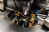
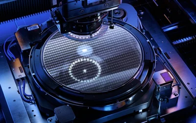
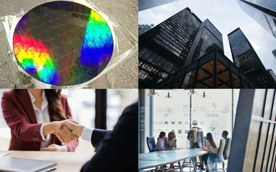
XIVER's Sreekanth Chirayath on why photonic innovations fail on the production line and how designing for manufacturing from the start changes the outcome.
XIVER's Sreekanth Chirayath on why photonic innovations fail on the production line and how designing for manufacturing from the start changes the outcome.
XIVER's Sreekanth Chirayath on why photonic innovations fail on the production line and how designing for manufacturing from the start changes the outcome.
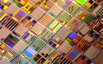
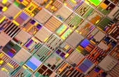
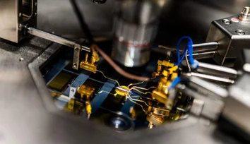
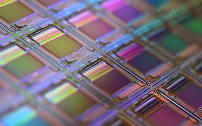
A discussion with New Origin CEO Twan Korthorst on why SiN is gaining popularity as an integrated photonics platform and how dedicated foundries can take PICs from prototype to production, creating new opportunities for startups and Global Photonics Engineering Contest 2026 participants.
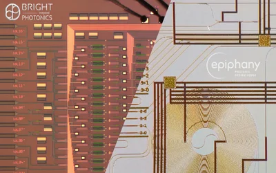
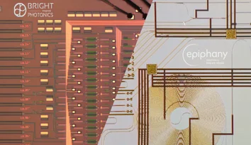
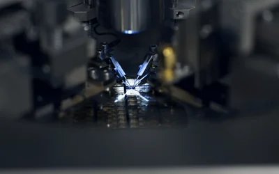
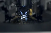
A Q&A with Epiphany Design and Bright Photonics on transforming PIC concepts into manufacturable systems, with practical guidance for teams participating in the Global Photonics Engineering Contest 2026.
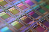
Photoresist, a light-sensitive material, is essential in photolithography for transferring intricate circuit patterns onto semiconductor wafers. This article explores positive vs. negative photoresists, detailing their chemical mechanisms, processing parameters, and performance traits.

Higher Education
ITMO University is one of Russia's leading higher education and research institutions, specializing in Information Technology, Opt...
17 Posts

Machinery Manufacturing
We Are Giving Human Materials the Superpowers of Nature Using Lasers
1 Post

XIVER's Sreekanth Chirayath on why photonic innovations fail on the production line and how designing for manufacturing from the start changes the outcome.
A discussion with New Origin CEO Twan Korthorst on why SiN is gaining popularity as an integrated photonics platform and how dedicated foundries can take PICs from prototype to production, creating new opportunities for startups and Global Photonics Engineering Contest 2026 participants.
A Q&A with Epiphany Design and Bright Photonics on transforming PIC concepts into manufacturable systems, with practical guidance for teams participating in the Global Photonics Engineering Contest 2026.
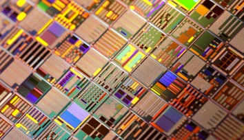
PhotonVentures explains how venture capital investors assess photonic chip startups, focusing on scalability, ecosystem alignment, and market readiness. They highlight key signals of investment readiness and the role of early validation opportunities like the Global Photonics Engineering Contest.
XIVER's Sreekanth Chirayath on why photonic innovations fail on the production line and how designing for manufacturing from the start changes the outcome.
A discussion with New Origin CEO Twan Korthorst on why SiN is gaining popularity as an integrated photonics platform and how dedicated foundries can take PICs from prototype to production, creating new opportunities for startups and Global Photonics Engineering Contest 2026 participants.
A Q&A with Epiphany Design and Bright Photonics on transforming PIC concepts into manufacturable systems, with practical guidance for teams participating in the Global Photonics Engineering Contest 2026.
PhotonVentures explains how venture capital investors assess photonic chip startups, focusing on scalability, ecosystem alignment, and market readiness. They highlight key signals of investment readiness and the role of early validation opportunities like the Global Photonics Engineering Contest.
Indium phosphide (InP) enables fully integrated photonic chips with high performance and efficiency. As an InP foundry, SMART Photonics supports the transition from design to scalable production through mature platforms and proven design flows.
How can photonic integrated circuits push the limits of sensing systems? Join PhotonDelta's Global Photonics Engineering Contest and develop sensing technologies of the future.
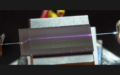
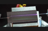
Sidewall-poled lithium niobate device paves way for compact UV sources
A new technique using ultrasound waves to activate light-emitting nanoparticles could be used to manipulate cell signals or facilitate light-based medical treatments in the future.
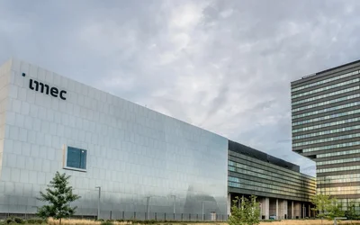
Datacom and AI infrastructure demands are rapidly driving the growth of integrated photonics. Philippe Soussan from imec explains his perspective on the recent developments and how he expects the industry to evolve in the next few years.
Insights into electro-optic frequency combs could lead to new applications

2 minutes read
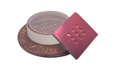
Learn how compact methane sensors use TDLAS, 1.6 µm detection, and InGaAs photodiodes to deliver stable, repeatable sub-ppm CH₄ measurements in industrial environments.
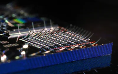
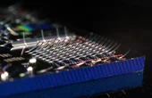
Light-emitting structures that curl off the chip surface could enable advanced displays, high-speed optical communications, and larger-scale quantum computers.
Caltech scientists have developed a way to guide light on silicon wafers with low signal loss approaching that of optical fiber at visible wavelengths.

4 minutes read
Innovative fabrication method for high-performance optical resonators
3 minutes read
Learn how photonic integrated circuits are reshaping the future of imaging, and why PhotonDelta is inviting engineers to rethink how PICs can tackle imaging challenges of today and power the next generation of innovation.