Engineering the Next Wave of Imaging with Photonic Integrated Circuits
Learn how photonic integrated circuits are reshaping the future of imaging, and why PhotonDelta is inviting engineers to rethink how PICs can tackle imaging challenges of today and power the next generation of innovation.

02 Mar, 2026. 8 minutes read
Imaging technologies enhance our living experience either by revealing the unseen or transforming the way we interact with the visible world. They help push the limits of human perception by detecting early-stage diseases, helping us understand underlying mechanisms in biological structures and shedding light on the vast mysteries of the universe. Beyond the sciences, imaging technologies enrich our day-to-day life, and now it has become feasible to make them more integrated than ever.
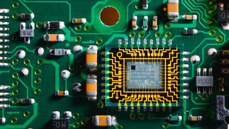
Today, after decades of research and technological achievement, it is now possible to develop photonic chips that precisely control light, unlocking advanced performance capabilities. Photonic Integrated Circuits (PICs) have allowed, in turn, for miniaturisation of discrete optical devices, have reduced energy consumption and overall footprint through the integration of components within a single fabrication process flow.
Current imaging systems are often bulky and expensive, making most of them unattainable by the public. With imaging playing a pivotal role in diagnostics, PICs are key to make diagnostics available to everyone. Recognising this potential, PhotonDelta is challenging the photonics community to shift its attention to producing new imaging technologies that leverage PICs.
PICs’ Special Architecture
With PICs, we can manipulate light in ways so that conventional optics, such as mirrors and lenses, can be replaced with on-chip elements, making them compact and light. The need for collimators diminishes as the waveguiding nature of PICs enables the light beam to propagate into various parts of the circuit. Careful alignment of the optical elements becomes a thing of the past, as light on the chip can be easily routed from one optical element to the next and propagated at any arbitrary angle through the waveguide, which is hardly achievable in bulk imaging systems.
Apart from optical elements, the miniaturisation of light sources and detectors can be achieved by co-integration with electronics, making PICs great candidates for complete on-chip imaging systems. Parts that would cost up to several thousand each can now be fabricated on chip, costing only $1 per mm2 in the case of volume manufacturing. The cost-control that PICs offers can transform imaging technologies into scalable systems that are affordable enough for everyone to access.
Let’s examine the imaging systems in which PICs hold the greatest potential for advancing innovation.
Imaging Applications Enabled by PICs
One of the few PIC imaging technologies that has seen commercial recognition is light detection and ranging, or LiDAR. Similar to its cousin technology, radar, LiDAR is used to visualise our surroundings. It does so by sending pulses of light that are then bounced off nearby objects before they are returned to the system. By recording the time-of-flight (TOF) of the light pulse, the distance to objects is known, and by two-dimensional scanning of space using these pulses, a 3D reconstruction of our environment can be built.
LiDAR has quickly become an essential element of autonomous driving systems (ADAS) in cars. LiDAR was once expensive and bulky, relying on moving parts to scan the environment, a design that severely limited its scalability. That’s where PICs come in, with their integration to LiDAR systems transforming the landscape.
PICs removed the need for rotating scanning parts that LiDAR used to consist of by implementing optical phased arrays (OPAs) or focal plane arrays (FPAs). These arrays can separate a laser source into distinct outputs that can travel in different directions, removing any additional beam steering parts. LiDAR in the automotive industry has allowed for a more stress-free driving experience, and other industries are looking to implement it in their technologies.
Another imaging application that can utilise PICs is augmented reality (AR), enabling user interaction with digitally enhanced environments. AR initially started as a tool to create immersive environments for the entertainment industry, but today, AR is used in many fields. In healthcare, surgeons use it to rehearse procedures before entering the operating room; in construction, it offers a visualisation of complex designs that 2D drawings simply cannot capture.
AR Technology has transformed enormously through the years, starting with head-mounted display systems and moving to AR glasses. Now, even designer eyewear has improved its AR technology to enhance the customer experience. The glasses are implemented with micro displays that project holograms. Not only are the users able to view the holograms, but they are also able to interact with them, enhancing the merged experience of physical and digital worlds.
This technology is currently focused on making the generated visuals even sharper, while miniaturising its components to extremely small sizes, making the frame even lighter. One promising application of PICs in modern AR technology is the development of energy-efficient, PIC-based RGB laser modules. These modules combine red, green, and blue laser sources onto a single photonic chip, enabling compact holographic projection systems that deliver vivid, high-quality imagery. This PIC design can be scaled by replicating other parts of an AR system on the same substrate, resulting in AR technologies that are less complex, more compact and scalable.
Another application where PICs are key to developing compact and affordable diagnostic imaging technologies is Optical Coherent Tomography (OCT). Currently, these systems involve expensive, bulky equipment and can be used only in a laboratory environment because they require operation by highly skilled scientists.
OCT, a technique widely used in diagnostic ophthalmology, requires expensive equipment that is highly sensitive to misalignment. The next generation of OCT devices needs to be miniaturised into a compact, low-cost and alignment-free system, which can potentially perform better than current OCT technologies. With modern medicine focusing on point-of-care practices, photonic chips are positioned to accelerate the widespread adoption of OCT devices, which have already been miniaturised to the size of a coin. By integrating key optical components onto a single chip, these devices can deliver diagnostic results faster, more reliably, and at a fraction of the cost of conventional systems. Designing new imaging systems with PIC technologies in mind can result in products that allow for minimally invasive diagnostics.
While PICs represent a transformative step forward in imaging technology, certain challenges remain. Areas such as chip fabrication precision, optical losses, and integration complexity are still being actively refined, with ongoing research dedicated to overcoming these hurdles.
Research Challenges and Engineering Trade-Offs
LiDAR
For ADAS LiDAR systems to achieve full integration in the automotive industry, several key challenges must be addressed. Those involve both system design and PIC-level challenges. From a system perspective, a design that considers both packaging and driving electronics requirements will ensure that ADAS LiDAR systems are widely adopted into future automobiles. System engineers need to take into account that the total package, including electronics and PIC components, does not exceed 35 Watt of power consumption. To image and reconstruct the surrounding environment, the ADAS LiDAR system needs to have a field of view of 30x120 degrees with an angular resolution of 0.05-0.01 degrees, while having a detection range of 300 meters. These requirements need to be met while keeping the overall system cost below €150, ensuring cost-controlled mass integration.
When it comes to the PICs themselves, further research and engineering are necessary to address the current shortcomings. For example, Silicon Nitride OPAs, a key PICs component for modern LiDAR technologies, suffer from an insertion loss of >13 dB, including the external lens that is used to collect light from the scene. OPAs can separate a laser source into distinct outputs that can travel in different directions, removing any additional beam steering parts. A modified design needs to be implemented, aimed at improving their current insertion loss.
To meet the high-resolution distance and velocity measurements, frequency-modulated continuous wave (FMCW) lasers are leveraged as they enable direct velocity measurement. However, their current design needs to be improved to ensure a stable operation across a wide range of frequencies, while also consuming low energy.
On-chip optical isolators are implemented to ensure the isolation between various optical components of the PIC systems, reducing optical feedback. They can make the design of the system more complex, resulting in packaging complications and contributing to loss. Engineering in this area should focus on designing on-chip isolators that are compatible with current requirements by considering new materials or even isolator-free PIC systems.
OCT
In OCT imaging, a 3D scan of an object is acquired, with 20 µm lateral and 5 µm vertical resolution. To ensure that photonic integrated OCT systems keep up with the current technological requirements, apart from resolution, their scan speed should be in the range of 100k points/scans per second, with a penetration depth of 5 mm for skin analysis and 1 mm for retina. Additionally, it is essential to ensure that the signal-to-noise ratio (SNR) of those systems doesn’t hinder their performance by achieving at least an SNR of 60 dB.
To meet those requirements, the PIC-OCT system takes inspiration from Fourier Domain techniques. By focusing on Fourier domain solutions, OCT can be put on a chip without sacrificing scanning speed or implementing moving components. In Spectral-Domain OCT (SD-OCT), a broadband source illuminates a sample, and the light response from interacting with the different layers of the sample is measured with an on-chip spectrometer. A second technique is Swept-Source OCT (SS-OCT), where a simple interferometer circuit is combined with a more complex light source. Both cases can be viable for high-speed, depth-resolved imaging, but the complexity of their circuits is significant and requires thorough tolerance analysis to reach scalability and become manufacturable products.
A major limitation for both techniques so far has been the need for mechanical beam scanning to build the sample’s image. In order to substitute mechanical galvo-scanners, researchers need to focus on beam steering methods that can steer the OCT beam to the sample without any moving parts. Lastly, the integrated light source needs to be stable across a wide range of wavelengths for a scan to avoid noise discrepancies.
AR
Current challenges that AR is facing are those of reducing the power consumption of the whole system. But apart from those, PIC-level engineering could result in the design of superior AR systems. While RGB lasers can sequence the required colours, eliminating the need for external filters, the standard digital micromirror device (DMD), an essential key component in AR responsible for controlling the hologram formation, needs to be substituted with an optical analogue. An ongoing challenge is to create a PIC-based beam steering chip to create and control the holographic projections while meeting specifications. For example, a resolution of 4M pixels, a field of view of 200 degrees, while working in the visible range, is essential to build AR systems that can compete with current technologies.
Another important challenge is how to reduce the cost of the glasses themselves while integrating diffractive optical elements into the lens. In AR glasses, the lens is not just a passive element; it is used to incorporate gratings or waveguides. To utilise them to their full potential, nanoimprinting techniques need to be employed to produce lenses with specific properties for the use case.
Overall, system-level engineering is needed to address these obstacles. Each application has specific priorities, and practical systems require balancing of parameters so PIC technologies can be at the forefront of innovation.
Lighting the Way to the Future of Imaging
Beyond entertainment and consumer applications, PIC-based imaging technologies hold transformative potential in healthcare, not only by miniaturising existing tools, but by enabling entirely new ones. They open the door to novel system architectures capable of powering next-generation devices, and may even lay the groundwork for quantum imaging techniques.
PhotonDelta invites innovators to confront the challenges still facing PIC technology and to help shape the future of imaging.
References:
Yusuke Kohno, Kento Komatsu, Rui Tang, Yasuyuki Ozeki, Yoshiaki Nakano, and Takuo Tanemura, "Ghost imaging using a large-scale silicon photonic phased array chip," Opt. Express 27, 3817-3823 (2019)
Giovanni Gilardi, Weiming Yao, Hadi Rabbani Haghighi, Xaveer J. M. Leijtens, Meint K. Smit, and M. J. Wale, "Deep Trenches for Thermal Crosstalk Reduction in InP-Based Photonic Integrated Circuits," J. Lightwave Technol. 32, 4262-4268 (2014)
de Cea Falco, Marc. "Integrated Photonics for Imaging: Novel Sources, Architectures and Applications. " Massachusetts Institute of Technology, (2024)
Vanuytsel, Steven, Quentin Desmeth, Victor Garcia-Munoz, Andim Stassen, Qingzhong Deng, Vittal Prakasam, Vladimir Leonov, Seungkyu Ha, Pol Van Dorpe, and Niels Verellen. "Lens-free photonic integrated circuit for sub-diffraction resolution and large field-of-view fluorescence imaging." In High-Throughput Biophotonics: Imaging, Spectroscopy, and Beyond X, p. PC133300K. SPIE, (2025)
Aaron Adkins, Senyue Hao, and Chao Zhou. "Photonic Integrated Circuits Enable High-Speed OCT Imaging of the Eye", Photonics Spectra, https://www.photonics.com/Articles/Photonic-Integrated-Circuits-Enable-High-Speed/a71109,(2025)