Photo Transistor – Comprehensive Guide for Modern Engineers
Learn everything about photo transistor devices, including working principles, types (BJT & FET), circuit design, key parameters, modes of operation, practical interfacing techniques, and modern applications.

14 Nov, 2025. 18 minutes read
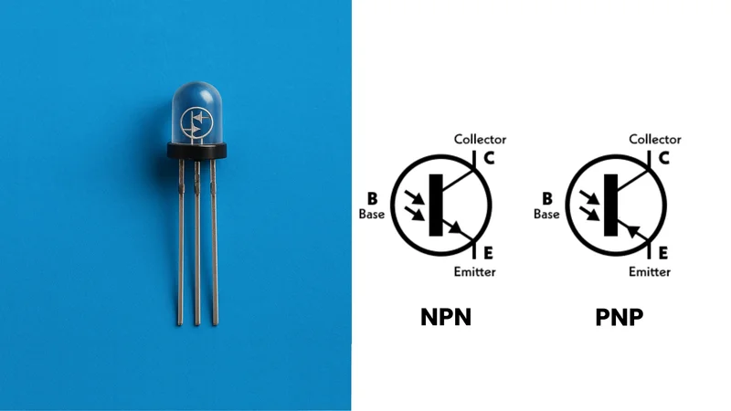
Photo Transistor - NPN, PNP Configurations
Key Takeaways
Enhanced Photocurrent: A photo transistor multiplies the photocurrent generated by a photodiode using transistor gain, producing collector currents hundreds or even thousands of times larger than a simple photodiode. This makes them easier to interface with digital logic or microcontrollers.
Two Major Types: Bipolar junction photo transistors (photo BJTs) are the most common and provide high gain but moderate speed; field‑effect photo transistors (photo FETs) offer higher switching speeds at the cost of lower gain.
Modes of Operation: By choosing the value of the load resistor, designers can use a photo transistor in active mode (analogue output proportional to light) or switch mode (digital on/off output).
Design Considerations: Key parameters include spectral response, dark current, response time, breakdown voltages, and temperature dependence. Selecting the proper transistor type, bias voltage, and load resistor is critical for reliable operation.
Typical Applications: Phototransistors appear in opto‑isolators, object detectors, encoders, security systems, remote controls, and opto‑digital interfaces. Modern heterojunction devices and photo FETs enable fast, sensitive detectors for visible and infrared light.
Introduction
Light detection plays a crucial role in modern electronic systems, enabling everything from counting optical encoder pulses to receiving infrared remote‑control signals. The photo transistor acts as both a light sensor and an amplifier, providing higher sensitivity than traditional photodiodes. Once photons strike the semiconductor junction, they generate charge carriers that are amplified by the transistor action, resulting in a stronger output signal. This makes the photo transistor ideal for applications such as infrared receivers, optocouplers, and light-controlled switches.
Invented in 1948 by John N. Shive, photo transistors produce much higher collector currents than photodiodes and are widely available today in through‑hole and surface‑mount packages. This article provides a detailed exploration of photo transistor technology, explaining its internal structure, working principles, types (BJT & FET), and circuit implementation techniques.
Phototransistor Fundamentals
Definition and History
Phototransistor is a semiconductor device that uses light instead of an electrical base current to control conduction between its collector and emitter. It can be viewed as a photodiode whose photocurrent is fed directly into the base of a bipolar transistor. When photons hit the light‑sensitive base–collector junction, electron–hole pairs are generated, and the resulting base current is amplified by the transistor, yielding a collector current proportional to the light intensity. Compared with photodiodes, phototransistors provide a current gain in the range of 10–1000.

John Northrup Shive invented the first phototransistor in 1948. He used a beam of light instead of a wire as the emitter of a point contact transistor, which generated holes that would flow to the collector. The success of his experiment led to the phototransistor, which Bell Telephone Laboratories announced on March 30, 1950. [1]
Early devices used homojunction silicon or germanium structures; modern high-performance devices employ heterojunctions using III–V materials, such as gallium arsenide (GaAs), to increase sensitivity. Although photodiodes remain popular for high‑speed analogue detection, phototransistors still thrive where on/off detection and large output currents are required.
Symbol and Physical Construction
Phototransistors typically come in two-lead or three-lead configurations.
Two-Lead Phototransistors expose only the collector and emitter, allowing automatic light control without external biasing.
Three-Lead Phototransistors include a base pin, enabling external biasing or sensitivity adjustment.
In circuit diagrams, the phototransistor symbol closely resembles that of a BJT, with arrows indicating incident light instead of an electrical base lead. In an NPN phototransistor, the emitter arrow points outward; in a PNP phototransistor, it points inward to denote current direction.

Physically, the base–collector junction is enlarged and encapsulated under a transparent epoxy lens that focuses incident light onto the base region. This structure increases photocurrent generation but also adds capacitance, which can slow response times. Designers must therefore balance gain, speed, and dark current when optimizing for specific light levels or ambient light conditions.
Modern high-speed variants use epitaxially grown layers and optical windows to minimize fall time and improve bandwidth. Overall, the phototransistor bridges optical sensing and electronic circuitry, combining the sensitivity of a photodiode with the amplification of a transistor amplifier, making it indispensable in today’s solid-state and optoelectronic designs.
Working Principle and Physics
Photovoltaic Effect and Current Amplification
The operating principle of a photo transistor is similar to that of a photodiode: incident photons generate electron–hole pairs in the depletion region of a reverse‑biased pn junction. In a phototransistor, the exposed region is the base of a bipolar transistor. The generated photocurrent serves as the input base current, which is multiplied by the DC gain (β) of the transistor. In other words:

where, Ic is the collector current, β is the current gain of the transistor, and Ip is the photocurrent. The current amplification allows phototransistors to produce collector currents in the milliamp range, orders of magnitude larger than typical photodiode currents.
One other way to conceptualise a phototransistor is as a photodiode driving the base of a transistor. The base–emitter junction is forward‑biased, while the base–collector junction is reverse‑biased. When light is absent, a small leakage current called "dark current" flows; this current depends on temperature. As the light intensity increases, the base current increases, and the collector current rises until the device saturates. The relationship between light intensity and collector current is linear only over 3–4 decades of illumination; at high light levels, the transistor’s gain decreases and linearity suffers.
Modes of Operation
Like conventional BJTs, phototransistors can operate in different regions of their output characteristics. In active (linear) mode, the collector current varies approximately linearly with light intensity, producing an analogue output. This mode is achieved when the load resistor is low enough so that the phototransistor does not saturate; the criterion is:

Because phototransistors are inherently nonlinear, the active mode is typically used for simple light‑level measurements rather than precision photometry.
In switch mode, the device functions as a digital on/off detector. When light intensity crosses a threshold, the phototransistor saturates and the collector–emitter voltage drops to a low value, often below 0.8 V. In the absence of light, the device is cut off and the output is pulled high through the load resistor. The switch mode is realised when:

typical designs use load resistors ≥ 5 kΩ. Opto‑isolators, encoders, and digital sensors often use phototransistors in switch mode.
Circuit Configurations
Two basic amplifier configurations are used to convert the photocurrent into a voltage: common‑emitter and common‑collector (emitter follower). [2]
In the common‑emitter configuration, the resistor is connected between the collector and the supply; the output is taken at the collector. Light causes the output voltage to drop from a high state toward ground.
The common‑collector configuration connects the resistor to the emitter, and the output is taken from the emitter; here, the output voltage increases with light intensity.
These simple circuits suffice for many applications. When linearity or speed is paramount, designers may use transimpedance amplifiers (TIAs) with photodiodes instead of phototransistors because TIAs provide a well‑controlled gain and wide bandwidth.
Recommended Reading: Types of Circuits: A Comprehensive Guide for Engineering Professionals
Types of Phototransistors
Bipolar Junction Phototransistors (Photo BJTs)
Bipolar junction phototransistors (photo BJTs) are the most widely used in modern electronic circuits. In an NPN photo transistor, the collector is biased positively relative to the emitter; in a PNP device, the collector is biased negatively. The base region is enlarged to collect photons and is either open (two‑lead devices) or connected to an external pin (three‑lead devices).
Photo BJTs offer high current gain, but their bandwidth is limited by the large base–collector capacitance; typical rise and fall times range from 1 µs to 10 µs. Devices configured as photodarlingtons, where a phototransistor drives an additional transistor, provide even higher gain but have slower response times in the 30–250 µs range.
The photodarlington connection multiplies the gains of two transistors. It is useful when tiny light signals must switch significant currents, for example, to drive relays or opto‑coupled outputs. However, the increased gain amplifies dark current and slows the device because the base–collector capacitance and stored charge are larger. Thus, photodarlington transistors are preferred in low-speed applications where gain is more critical than speed.
Field‑Effect Phototransistors (Photo FETs)
Field-effect phototransistors (photo FETs) replace the bipolar transistor with a field-effect transistor, such as a JFET or MOSFET. In these semiconductor devices, the light-sensitive region lies within the channel between the drain and source, while the gate remains shielded from light. Depending on the structure, photo FETs can operate with n-channel or p-channel conduction and may employ enhancement-mode or depletion-mode operation.

FETs require no base current for control, so photo FETs exhibit lower input noise, reduced dark current, faster response times, and improved high-speed switching characteristics. They excel in high-frequency or low-light detection applications such as optical encoders, light meters, and data communication systems.
Homojunction vs Heterojunction Structures
The structural composition of a phototransistor greatly affects its spectral response and performance characteristics.
Homojunction Phototransistors are made from a single semiconductor material (such as silicon or germanium). They are cost-effective and provide moderate gain (≈ 50–500) with response times suitable for general light-sensing applications.
Heterojunction Phototransistors, by contrast, employ multiple semiconductor materials with differing band gaps, typically III–V compounds like gallium arsenide (GaAs), indium gallium arsenide (InGaAs), or lead sulfide (PbS). These materials extend wavelength sensitivity, reduce dark current, and improve amplification efficiency.
Modern heterojunction phototransistors offer responsivity and current gain up to 10,000, making them highly effective for high-speed optical sensing, infrared spectroscopy, and precision light measurement systems.
Recommended Reading: Understanding JFET Technology: Applications and Misconceptions
Key Electrical Characteristics
When selecting a photo transistor, designers must consider several parameters that influence performance:
Spectral Response and Sensitivity
The spectral response describes how the detector’s output varies with wavelength. Phototransistors respond over a broad range from near‑ultraviolet to near‑infrared (e.g., 700–1100 nm). The peak responsivity usually occurs in the near‑infrared at ≈840 nm. To maximise signal, many devices are matched to IR LEDs at 880–940 nm. The base area and transistor gain determine the responsivity; doubling the base area doubles the generated photocurrent. However, increasing the area also increases capacitance and reduces speed.
Sensitivity refers to the ratio of change in collector current to change in light intensity. High sensitivity is desirable for detecting slight variations in light. Sensitivity increases with gain and area but is limited by dark current and noise. The dark current flows even when no light is present; typical values range from 10 nA to 100 nA at room temperature. To reduce dark current, some devices include a base–emitter resistor in three‑lead configurations.
Linearity and Dynamic Range
Phototransistors exhibit poorer linearity than photodiodes because their current gain decreases at high collector current levels. The relationship between light intensity and collector current remains approximately linear over three to four decades of illumination.

For high-accuracy measurements across a broad dynamic range, photodiodes with transimpedance amplifiers (TIAs) are preferred, as they maintain predictable gain and bandwidth. Conversely, phototransistors excel as light-controlled switches in digital or threshold-based sensing applications.
Response Time and Bandwidth
The response time (rise and fall time) of a phototransistor is dominated by the base–collector capacitance and the load resistance. Due to the Miller effect, higher current gain (β) amplifies this RC constant, slowing down the transient response. Typical rise/fall times range from 1–10 µs for standard photo BJTs, while photodarlington configurations are slower (30–250 µs) because of additional junction capacitance and charge storage.
By contrast, photo FETs and avalanche photodiodes can achieve nanosecond-level response times, though with lower amplification. For applications requiring high bandwidth, designers should minimize load resistance or select low-capacitance phototransistors to reduce RC delays.
Breakdown Voltages
Phototransistors have maximum allowable collector–emitter and emitter–collector breakdown voltages. Exceeding these values causes permanent damage. Typical devices tolerate 20–50 V across the collector–emitter junction and 4–6 V across the emitter–collector junction. Designers usually operate at low voltages (5 V) to avoid breakdown and minimise dark current.
Temperature Dependence
Temperature significantly influences both gain (β) and dark current (Id). Once the temperature rises, dark current increases exponentially due to enhanced carrier generation, while gain typically decreases because of higher recombination rates in the base region. The combined effect reduces sensitivity and may shift the operating point of the circuit.
For applications exposed to large temperature variations, designers often include temperature compensation or periodic calibration to maintain accuracy. In field-effect phototransistors, additional bolometric effects, where temperature changes alter the channel resistance, can appear at longer wavelengths; distinguishing them from purely photovoltaic behavior.
Modes of Operation and Design Equations
Phototransistor circuits are simple, but obtaining reliable performance requires selecting the correct mode and resistor values.
Active Mode
In active (analog) mode, the output voltage varies proportionally with light intensity, producing a continuous analog signal. To maintain linearity, the load resistor must be small enough to prevent the phototransistor from saturating. The condition for linear operation is:

Here, Vcc is the supply voltage, R(L) is the load resistance, and Icc is the maximum anticipated collector current under illumination. For example, a phototransistor with Icc ≈ 4 mA and Vcc = 5 V yields:

To provide margin and maintain linearity, choose a resistor about 30% lower (≈ 820 Ω).
In this mode, the collector current increases with illumination, and the output voltage decreases correspondingly. The transfer curve is nonlinear: collector current rises steeply at low light levels and saturates at high illumination. Hence, active mode suits applications like light meters, solar trackers, and illumination monitors, where approximate intensity readings are acceptable.
Switch Mode
For digital detection, the circuit should transition cleanly between off and on states. In switch mode, the load resistor is large enough that the phototransistor saturates when exposed to light. The design equation is:

The rule of thumb is to use R(L) ≥ 5 kΩ to ensure saturation. The high‑level output should be close to Vcc, and the low‑level output should be below 0.8 V. Digital logic inputs typically recognise voltages < 0.8 V as logic low when powered at 5 V.
Switch mode is used in encoders, opto‑isolators, counters, and photointerrupters. Because the phototransistor saturates, the turn‑off time can be slower than the turn‑on time, especially for photodarlingtons.
Base Bias and Sensitivity Control
Three-lead phototransistors allow designers to connect a base–emitter resistor for sensitivity adjustment and dark current reduction. The higher base–emitter resistor value decreases dark current, prevents false triggering from low ambient light, and raises the threshold light level needed for conduction. [3]
By biasing the base slightly negative relative to the emitter, the base–emitter resistor effectively reduces gain (β) and makes the output response more digital. This feature is valuable when designing circuits that must reject weak or fluctuating light signals, ensuring consistent performance under varying illumination conditions.
Recommended Reading: Optical Encoder Technology: Advanced Guide to Precision Motion Control Systems
Practical Design and Interfacing
Selecting the Right Phototransistor
When choosing a photo transistor for a project, consider the following steps:
Determine Wavelength Range and Spectral Match: Select silicon devices for 190–1100 nm or InGaAs devices for longer wavelengths. Match the peak response to the light source (e.g., 880 nm IR LED). Use optical filters if ambient light interference is problematic.
Assess Required Gain and Speed: Choose a photo BJT for high gain; choose a photo FET for faster response. For extremely weak light signals or high output currents, use a photodarlington or an avalanche photodiode followed by an amplifier.
Check Collector Current and Breakdown Voltage: Ensure the device can handle the expected collector current and operate within the supply voltage. Many surface‑mount phototransistors are rated for only a few milliamps and breakdown voltages around 30 V.
Consider Package and Optical Geometry: For side‑looking detection, use side‑view packages; for axial detection, use through‑hole packages with lenses. Ensure the mechanical design aligns the light path with the sensitive area.
Biasing and Resistor Selection
Bias Voltage: Phototransistors typically operate from 3–5 V in digital logic circuits or up to 15 V in analogue circuits. Higher voltages slightly increase gain but also increase dark current and the risk of breakdown.
Load Resistor: Use the design equations to determine R_L. For example, suppose a 5 V supply and a phototransistor rated for Icc = 2 mA. For switch mode, choose R(L) ≥ 5 kΩ so that Vcc < R(L) × Icc (5 V < 5 kΩ × 2 mA = 10 V), ensuring saturation. For active mode, choose R(L) smaller than 5 V/2 mA = 2.5 kΩ. Many microcontroller circuits use 1 kΩ – 10 kΩ resistors.
Base Bias Resistor: If using a three‑lead device, add base bias resistor (typically 100 kΩ) between base and emitter to reduce dark current and noise. Avoid connecting the base pin directly to a logic voltage without a resistor, as this will cause it to behave like a normal transistor rather than a phototransistor.
Interfacing with Microcontrollers
Phototransistors can easily interface with microcontrollers using either analogue or digital inputs. Here is a common procedure:
Connection Configuration: Connect the collector to Vcc through the load resistor (common‑emitter) or connect the emitter to ground through the resistor (common‑collector).
Microcontroller Input: Connect the non‑resistor terminal to the microcontroller input. For analogue measurement, connect to an ADC pin; for digital measurement, connect to a GPIO configured as an input.
Example Implementation: Choose R(L) and Vcc based on whether a digital or analogue output is desired. For example, an Arduino project used a 1 kΩ resistor between the phototransistor emitter and ground, and connected the collector to 5 V. The microcontroller then read the voltage across the resistor to measure light intensity. The code simply read the ADC value and scaled it back to voltage.
Signal Filtering and Debouncing: To suppress noise from flicker or ambient light, use a simple RC filter or apply software averaging. For digital applications, use Schmitt trigger inputs or comparators (e.g., LM393) to shape clean transitions.
Dealing with Nonlinearity and Temperature Effects
To improve linearity, limit the input light intensity range or apply software calibration. In digital applications, nonlinearity is rarely problematic since the phototransistor saturates fully under illumination.
For temperature variation, measure ambient temperature and adjust thresholds or gain compensation dynamically. Alternatively, use phototransistor packages with integrated temperature compensation or photo FETs, which are less sensitive to thermal drift.
Safety and Isolation
Phototransistors are integral components in opto-isolators, providing galvanic isolation between circuits. When designing isolation stages:
Verify that the breakdown voltage and creepage distances meet relevant safety standards.
Avoid operating near maximum ratings; derate the voltage by 20–30% to ensure reliability.
Include protective diodes or snubbers across the collector–emitter junction to suppress transient voltages and prevent avalanche breakdown.
Applications
Phototransistors are versatile components. The common uses include:
Opto-Isolators / Optocouplers
In an opto-isolator, an infrared LED transmits light across an insulating gap to a phototransistor receiver. [4] The collector current generated by the phototransistor reproduces the input signal while maintaining galvanic isolation between high- and low-voltage circuits. The phototransistor typically operates in switch mode, saturating to represent digital logic levels. The applications include microcontroller interfaces, switch-mode power supplies, and communication links, where safety and noise immunity are critical.
Object Detection and Photo-Interrupters
Photo-interrupters employ a U-shaped housing that contains an IR-LED on one side and a phototransistor on the opposite side. Once an object obstructs the light beam, the phototransistor turns off, generating a clear digital output change. These devices are common in printers, disk drives, and industrial counting systems. For consistent operation, designers ensure correct optical alignment, minimize ambient light interference, and often include Schmitt trigger conditioning for clean signal edges.
Encoders and Counters
Rotary and linear encoders use arrays of phototransistors aligned with slotted discs or gratings. Once light passes through the slots, the phototransistor switches rapidly between ON and OFF states, producing pulse trains. Operating in switch mode provides precise digital transitions for position and speed detection. Encoders often pair photo BJTs or photo FETs with comparator circuits to enhance bandwidth and reduce noise.
Remote Control Receivers
In infrared remote control systems, the phototransistor acts as a primary light sensor. It detects modulated IR signals (typically 36–40 kHz) transmitted from handheld remotes. Its high amplification allows detection of low-power signals across several meters. The phototransistor output is filtered and processed by an integrated amplifier or demodulator IC to decode the data. To reject ambient light, most receivers use optical filters centered on the IR wavelength band.
Security Systems and Motion Detectors
Phototransistors are integral to IR beam sensors used in security alarms and automatic door systems. Once the infrared beam between transmitter and receiver is interrupted, the collector current drops sharply, triggering a control signal. Paired with comparators or op-amps, these devices provide reliable intrusion detection. Photodarlington versions are often used to extend detection range in low-light or long-distance conditions.
Light-Controlled Switches
In automatic lighting and energy-saving systems, phototransistors serve as light-controlled switches. They detect ambient light levels and toggle relays, lamps, or motors accordingly. Photodarlington configurations are particularly useful here, providing high current gain to drive loads directly. Designers commonly add hysteresis or feedback via comparators to prevent oscillation near the threshold.
Pulse Oximeters and Biomedical Sensors
In biomedical instrumentation, phototransistors detect transmitted or reflected light through biological tissue. Paired with LEDs of different wavelengths, they measure variations in light absorption corresponding to oxygenated and deoxygenated hemoglobin. The resulting signal is amplified and filtered for pulse oximetry and heart-rate monitoring. Here, low dark current and stable gain across temperature variations are essential for accuracy.
Data Transmission and Optical Links
While photodiodes dominate high-speed communication due to superior bandwidth, phototransistors remain suitable for low-speed optical data links. They can decode optical pulses in industrial control and short-range communication systems where simplicity outweighs speed. However, for data rates above a few hundred kilohertz, designers prefer photo FETs or avalanche photodiodes for improved response time and linearity.
Specialized Uses
Beyond conventional electronics, phototransistors also appear in astronomical instruments, night-vision sensors, and IR imaging systems. Their high responsivity in the infrared spectrum makes them ideal for detecting faint celestial sources or environmental light variations. The careful biasing, temperature compensation, and optical calibration allow such sensors to operate reliably across extreme environmental conditions.
Recommended Reading: The Optoelectronics Behind Factory Automation
Phototransistor vs. Alternative Detectors
Comparison with Photodiodes
Both photodiodes and phototransistors convert light into current, but their characteristics differ. Photodiodes produce linear, fast, and low‑current outputs; phototransistors provide amplified outputs but with non‑linearity and slower response.
| Parameter | Photodiode | Phototransistor |
| Terminals | Two (anode and cathode) | Two or three (collector, emitter, optional base) |
| Current gain (β) | 10–150 | 10–1000 |
| Sensitivity | Low | 100× higher than a photodiode |
| Response Time | Fast (nanoseconds) | Slow (microseconds) |
| Dark Current | Lower | Higher |
| Linearity | Excellent over 7–9 decades | Limited to 3–4 decades |
| Preferred Use | Precise light measurement, high‑speed communication | On/off detection, when high output current is needed |
In summary, photodiodes are ideal for high-speed and precision measurements, while phototransistors excel in cost-effective, logic-level, or threshold-based sensing applications where amplified current output is more valuable than high linearity.
Advantages and Disadvantages of Phototransistors
Advantages
High Responsivity: Offer current gains up to 1500, providing much higher output current than photodiodes.
Compact and Low-Cost: Simple structure and integration make them suitable for mass production.
Broad Spectral Sensitivity: Detect light across UV, visible, and IR ranges; compatible with light sources from LEDs to sunlight.
Ease of Interfacing: Can directly drive microcontroller inputs or logic circuits without external amplifiers.
Versatile Packaging: Available in through-hole, SMD, and optically filtered variants, with GaAs-based models supporting higher voltages.
Stability: Exhibit long-term temporal stability and low noise when properly biased.
Disadvantages:
Slower Response: Typical response times are in microseconds, slower than nanosecond-level photodiodes.
Limited Linearity: Gain decreases at high collector currents, reducing accuracy in analog measurement.
Higher Dark Current: Leakage current increases with temperature, affecting precision at low light levels.
Restricted Bandwidth: Unsuitable for high-frequency or optical communication systems.
Voltage Sensitivity: Limited to moderate operating voltages and prone to voltage spikes in power circuits.
Reduced Low-Light Performance: Cannot detect extremely weak illumination as efficiently as avalanche photodiodes or PIN photodiodes.
Phototransistors vs Photoresistors and Avalanche Photodiodes
Photoresistors (LDRs)
Photoresistors, or light-dependent resistors, are passive sensors whose resistance decreases as light intensity increases. While inexpensive, they suffer from poor linearity and slow response times (typically 10–100 ms). Phototransistors outperform LDRs by offering microsecond-scale switching and far higher sensitivity, making them suitable for digital and real-time optical sensing.
Avalanche Photodiodes (APDs)
Avalanche photodiodes achieve extreme sensitivity and bandwidth by using avalanche multiplication of carriers under high reverse bias (typically 100–400 V). They are favored in fiber-optic communications, LiDAR, and laser-ranging systems, but require precise bias control and exhibit noise that scales strongly with bias voltage. Phototransistors, by contrast, operate at low voltages (3–15 V), provide moderate gain, and maintain lower noise, making them simpler and safer for general-purpose applications.

In essence, phototransistors occupy a practical middle ground among light sensors, offering a robust balance of sensitivity, simplicity, and integration flexibility for medium-speed, high-responsivity designs.
Emerging Technologies and Future Directions
Heterojunction and CMOS Integrated Phototransistors
Modern heterojunction phototransistors (HPTs) based on compound semiconductors such as gallium arsenide (GaAs) and indium gallium arsenide (InGaAs) are achieving unprecedented responsivity and extended infrared sensitivity. These devices can deliver current gains exceeding 10,000 and operate efficiently at wavelengths up to 2.6 µm. [5]
Integration of phototransistors into CMOS fabrication processes enables fully monolithic light sensors and optical receivers that coexist with digital and mixed-signal circuitry on the same chip.

Advanced CMOS image sensors now incorporate phototransistor-based pixels for near-infrared (NIR) imaging, providing high signal-to-noise ratios and compatibility with standard electronics manufacturing. This integration bridges the gap between discrete optoelectronic components and system-on-chip architectures.
Photo FETs and Bolometric Detectors
Research into field-effect phototransistors (photo FETs) is expanding rapidly. Unlike bipolar phototransistors, these devices rely on photogenerated charges that modulate the channel conductivity, eliminating the need for the base current. The result is higher switching speed, lower input noise, and improved temperature stability. Photo FETs are increasingly adopted in high-speed photonic integrated circuits (PICs) and data communication systems, where bandwidth and response time are critical.
Some photo FET architectures exploit bolometric effects, where light-induced heating alters channel resistance rather than generating carriers. Such hybrid bolometric-photoconductive mechanisms open possibilities for broadband detection extending from visible to mid-infrared ranges.
Novel Materials and Nanostructures
The next generation of phototransistors is emerging from research into low-dimensional materials and quantum nanostructures. Materials such as graphene, transition-metal dichalcogenides (TMDs) like MoS₂ and WS₂, and perovskite semiconductors offer ultrahigh carrier mobility, atomic-scale tunability, and broad spectral responsiveness. Their bandgaps can be engineered to target specific wavelengths, while maintaining low dark current and high gain.
Nanostructured devices: including nanowire phototransistors, quantum-dot phototransistors, and hybrid perovskite-silicon detectors, promise significant improvements in gain-to-noise ratio, power efficiency, and tunable spectral response. These developments aim to combine the best features of photodiodes, photo FETs, and traditional phototransistors into a single compact platform.
Recommended Reading: Concurrent-Mode CMOS Detector IC for Sub-Terahertz Imaging System
Conclusion
Phototransistors remain indispensable in modern optoelectronics, offering a practical balance between sensitivity, simplicity, and integration. By combining the photovoltaic effect with inherent transistor amplification, they enable direct light detection and signal driving without complex circuitry. Understanding their types, gain characteristics, and biasing equations allows engineers to tailor designs for either analog or digital operation. Though slower and less linear than photodiodes, their high responsivity and low-cost versatility sustain their dominance in opto-isolators, encoders, and light-controlled systems. With ongoing advances in heterojunctions, CMOS integration, and nanomaterials, phototransistors are poised to evolve into even more sensitive, efficient, and compact solutions for robotics, automation, and smart sensing applications.
Frequently Asked Questions (FAQs)
Q. What is the basic difference between a photodiode and a phototransistor?
A. The photodiode produces a small current proportional to light and must be amplified externally. On the other hand, a photo transistor integrates a transistor amplifier, resulting in collector currents hundreds or thousands of times larger. However, phototransistors are slower and less linear than photodiodes.
Q. Why is my phototransistor output noisy?
A. Noise can originate from ambient light, supply ripple, base–collector capacitance, or the ADC in microcontroller. Reduce it by shielding, using optical filters, lowering load resistor, adding RC filters, or including a base–emitter resistor to suppress dark current.
Q. Can phototransistors detect infrared light?
A. Yes. Silicon phototransistors respond to wavelengths from ≈190 nm to ≈1100 nm, with peak responsivity around 840 nm. Devices made of GaAs or InGaAs extend sensitivity further into the near‑IR (up to 2600 nm). Many commercial phototransistors are optimised for 880–940 nm to match IR LEDs.
Q. Do I need a base pin on a phototransistor?
A. Two‑lead phototransistors omit the base pin and operate solely via incident light. Three‑lead devices include a base pin that can be biased to adjust sensitivity or add a resistor to reduce dark current. For most applications the base pin is left open; use it only if you need to fine‑tune sensitivity.
Q. How can I improve the speed of a phototransistor circuit?
A. Reduce the load resistance to decrease the RC time constant, choose a phototransistor with a small collector‑base capacitance, use a photo FET instead of a BJT, or switch to a photodiode with a transimpedance amplifier. Avoid photodarlingtons if speed is critical because they have slower response times (30–250 µs).
References
[1] EDN. Bell Labs announces the Phototransistor, March 30, 1950 [Cited 2025 November 10] Available at: Link
[2] Semi. Optoelectronic Sensors - Chapter 4: Phototransistors [Cited 2025 November 10] Available at: Link
[3] EDN. Design Fundamentals for Phototransistor Circuits [Cited 2025 November 10] Available at: Link
[4] RP Photonics. Opto Isolators [Cited 2025 November 10] Available at: Link
[5] Research Gate. InGaP/GaAs Heterojunction Phototransistors for Ultra-low Optical Power Detection [Cited 2025 November 10] Available at: Link
in this article
1. Key Takeaways2. Introduction3. Phototransistor Fundamentals4. Working Principle and Physics5. Types of Phototransistors6. Key Electrical Characteristics7. Modes of Operation and Design Equations8. Practical Design and Interfacing9. ApplicationsPhototransistor vs. Alternative Detectors11. Emerging Technologies and Future Directions12. Conclusion13. Frequently Asked Questions (FAQs)14. References