Understanding JFET Technology: Applications and Misconceptions
Looking closely at the role of JFET Technology in modern electronics and debunking common myths.

08 Apr, 2025. 6 minutes read
Junction Field-Effect Transistors (JFETs) have been essential components in low-noise, high-impedance, and precision analog circuits for decades. Whereas bipolar junction transistors (BJTs) require base current for operation, JFETs are distinguished as voltage-controlled devices that regulate current through a depletion-mode conduction channel. Their high input impedance, low noise, and predictable behavior have made them an excellent choice for applications like sensor front-ends, audio preamplifiers, and scientific instrumentation.
Despite the dominance of Metal-Oxide-Semiconductor Field-Effect Transistors (MOSFETs) in digital and power electronics, JFETs remain integral in applications where signal integrity and stability outweigh switching speed and power efficiency. The misconception that JFETs are obsolete or inefficient ignores their exceptional performance in analog designs, where they outperform MOSFETs in noise-sensitive and high-impedance applications. This article explores the fundamentals of JFET operation, their electrical characteristics, practical applications, and dispels some common misconceptions that have led to their unfortunate underuse.
JFET Structure and Operating Principles
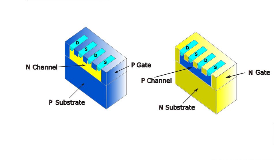
A JFET consists of a source, drain, and gate, with a conduction channel between the source and drain. The gate forms a reverse-biased PN junction with the channel, which creates a depletion region that restricts current flow. In contrast to MOSFETs, which use an insulated gate to control conduction, JFETs operate entirely through junction depletion, which makes them inherently normally-on devices.
An N-channel JFET, which relies on electron conduction, typically exhibits higher transconductance and lower ON resistance than a P-channel JFET, which relies on hole conduction. The difference in carrier mobility between electrons and holes results in N-channel JFETs offering approximately twice the transconductance of their P-channel counterparts for the same geometry and operating conditions.
The operation of a JFET is governed by the voltage applied between the gate and source (VGS). When VGS is zero, the depletion region is minimal, and the device allows maximum current flow between drain and source. As a negative bias is applied to the gate (for an N-channel JFET), the depletion region expands and reduces the available conduction path. When VGS reaches the pinch-off voltage (VP), the channel is fully depleted, and the drain current approaches zero. This depletion-mode behavior allows JFETs to function as voltage-controlled resistors.
The relationship between drain current (ID) and gate voltage follows a quadratic law:
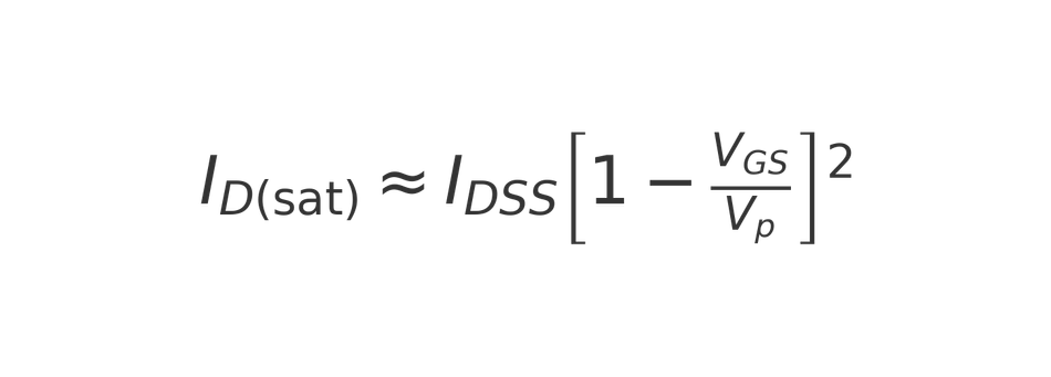
where IDSS is the maximum drain current at VGS = 0. This quadratic dependence results in smooth gain control, which is desirable in low-distortion amplifiers and RF attenuators.
Meanwhile, the drain-source voltage (VDS) determines the operating region of the JFET. In the ohmic region, where VDS is small, the JFET behaves as a voltage-controlled resistor with a resistance that varies with VGS. In the saturation region, where VDS exceeds the pinch-off point, the current stabilizes and becomes largely independent of VDS, making this region ideal for amplification. Beyond the breakdown voltage, excessive drain-source voltage causes avalanche conduction that leads to uncontrolled current flow and potential device failure.
Electrical Characteristics and Performance
Input Impedance and Leakage Currents
The input impedance of a JFET is typically in the range of 10⁹ to 10¹² Ω, which is orders of magnitude higher than that of a BJT. This ultra-high impedance helps JFETs in applications where sensor loading must be minimized, such as pH meters and charge amplifiers for photodetectors. Gate leakage current is usually below 10 pA at room temperature and remains low even as temperature increases, unlike MOSFETs, which suffer from oxide leakage currents.
Noise Performance
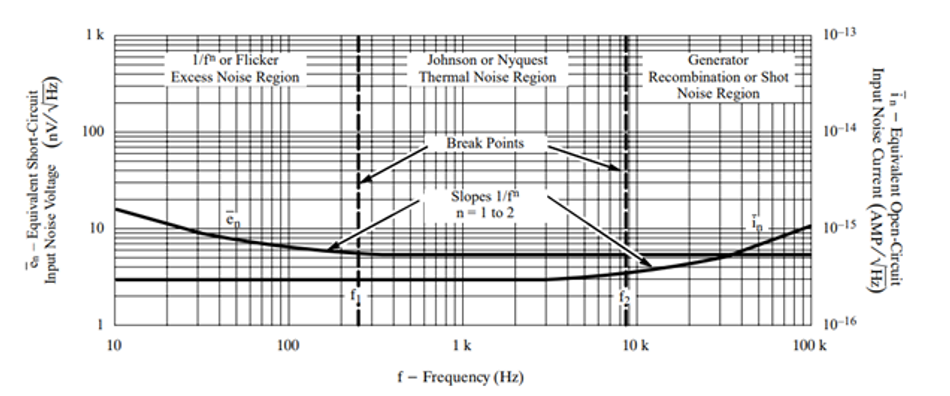
The noise performance of JFETs surpasses that of both BJTs and MOSFETs in low-frequency and high-impedance applications. The 1/f noise corner frequency of a JFET is typically below 100 Hz, significantly lower than MOSFETs, which often exhibit higher flicker noise due to trapping effects in the gate oxide. In the thermal noise regime, JFETs introduce less noise than BJTs because they do not require a base current, which eliminates shot noise contributions. This combination of low 1/f and thermal noise makes JFETs the preferred choice for ultra-low-noise front-end amplifiers.
<grammarly-extension></grammarly-extension><grammarly-extension></grammarly-extension><grammarly-extension></grammarly-extension><grammarly-extension></grammarly-extension>
JFET vs. MOSFET: Performance Trade-Offs
MOSFETs offer higher input impedance due to their insulated gate but suffer from higher off-state leakage currents and greater gate capacitance. A MOSFET with an input capacitance of 50 pF will exhibit an input impedance drop of over 300 kΩ at 10 MHz, whereas a JFET with a gate capacitance of 5 pF retains impedance in the tens of megaohms. The lower capacitance of JFETs makes them superior in high-impedance RF front-end circuits and low-noise signal processing.
Applications of JFETs
Low-Noise Signal Amplification
JFETs dominate audio preamplifiers, hydrophone amplifiers, and electrometers since minimizing input noise is paramount. In microphone preamplifiers, a low-noise JFET can achieve an equivalent noise voltage of less than 1 nV/√Hz, comparable to the best vacuum tube circuits in high-fidelity audio.
Precision Analog Circuits
JFETs are essential in instrumentation amplifiers and high-impedance buffer circuits. An oscilloscope probe using a JFET-input buffer can maintain 10 MΩ impedance while driving a 50 Ω system.
Analog Switching and Voltage-Controlled Resistance
JFETs function as low-charge-injection analog switches, with leakage currents below 100 pA. This lets them outperform MOSFET switches in sample-and-hold circuits where charge injection can introduce errors in high-resolution ADC systems.
Radiation-Hardened and High-Temperature Electronics
JFETs tolerate total ionizing radiation doses above 100 krad without performance degradation. This superior performance to MOSFETs makes them a great choice in space applications and nuclear instrumentation. Meanwhile, their thermal stability allows operation in environments exceeding 175°C, where MOSFETs suffer from threshold voltage shifts.
Misconceptions About JFETs
Unfortunately, many misconceptions about JFETs have led to their continual underuse in modern circuits. We will now dispel a number of these misconceptions.
Misconception #1: JFETs Are Obsolete
JFETs are widely used in low-noise and precision applications due to their high input impedance, negligible gate current, and excellent low-frequency noise performance. Unlike bipolar transistors, JFETs introduce minimal current noise, allowing them to pair well with high-impedance sources like photodiodes and piezoelectric sensors. These features, along with stable noise performance and ESD-resiliency, keep them relevant in modern op-amps, RF circuits, and sensor interfaces.
Misconception #2: JFETs Are Inefficient
While MOSFETs are optimized for switching applications, JFETs operate with near-zero gate current and can be biased to minimize temperature drift. This feature makes JFETs highly efficient in low-power precision applications.
Misconception #3: JFETs Are Too Fragile
JFETs exhibit higher ESD tolerance than MOSFETs. The oxide layer in MOSFETs is inherently fragile. The PN junction in JFETs has superior ESD performance & radiation tolerance. This makes them highly reliable in space and military electronics
Misconception #4: JFETs Are Too Complex
One common misconception is that JFETs are difficult to design with compared to MOSFETs. In reality, JFETs often require less protection circuitry due to their gate characteristics as noted above. This reduces the need for external protection diodes or gate resistor networks and effectively simplifies circuit design.
Design Considerations and Selection Criteria
Clearly, JFETs are the preferred choice in low-noise, high-impedance, and precision analog applications. JFETs are not intended to be the choice for high-power switching applications. While SiC JFETs exist for power applications, MOSFETs and IGBTs remain superior for high-voltage and high-current applications. Circuits that require enhancement-mode behavior, such as logic-level switching and digital applications, favor MOSFETs due to their normally-off state and lower gate drive requirements.
While JFETs offer excellent low-noise and high-impedance performance, their parameter variation across manufacturing batches is a challenge the manufacturer needs to consider. Fortunately, InterFET's close alignment with their foundry partners helps ensure customers' specs are met across all manufacturing lots. These challenges can also be mitigated by choosing matched JFET pairs or implementing negative feedback loops to stabilize performance in amplifier designs.
JFET Design Tips
Biasing a JFET requires setting the gate-source voltage (VGS) appropriately to control the drain current. Where MOSFETs can be directly driven from a logic-level signal, JFETs require negative gate biasing (for N-channel devices) to regulate conduction. Self-biasing techniques, such as using a source resistor to establish a stable operating point, simplify design and compensate for variations in IDSS (drain-source saturation current).
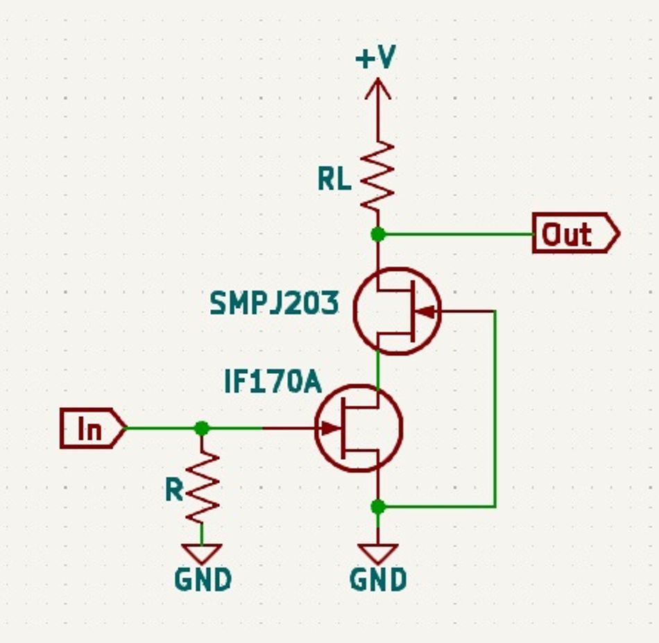
JFETs also benefit from cascode configurations, which improves gain stability, bandwidth, and linearity in precision analog and RF circuits. In a JFET cascode, a common-source JFET stage is stacked with a common-gate JFET or MOSFET, effectively isolating the input-dependent Miller capacitance from the output. By maintaining a nearly constant drain-source voltage on the lower JFET, gain variations due to channel-length modulation are reduced and signal integrity is improved. This configuration reduces parasitic feedback and extends the high-frequency response beyond what a single-stage JFET amplifier could achieve.
Conclusion
JFETs remain indispensable in modern low-noise, high-impedance, and radiation-tolerant applications. Their superior noise performance, stable input characteristics, and reliability in extreme environments make them a preferred choice in high-fidelity audio, scientific measurement, and space electronics. While MOSFETs have replaced JFETs in power and digital circuits, the precision analog domain continues to depend on JFETs for their unmatched signal integrity and reliability. Understanding their unique strengths and correct implementation will help JFETs remain an essential part of modern analog design.
References
- MOSFETs vs JFETs: Understanding Structures, Differences & Applications
- JFET Application Note
- Siliconix JFET Application Note AN101
- Siliconix JFET Application Note AN106