
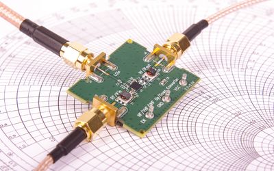
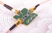
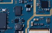
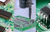
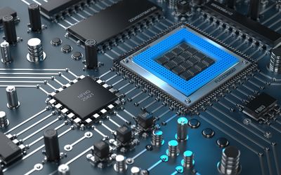
This article delves into the world of RF PCBs, exploring the design considerations that ensure signal integrity, the materials that minimize signal loss, and the intricate processes that bring these high-performance boards to life.
Be the first to know.
Get our pcb weekly email digest.
Tagged with
PCB
ORGANIZATIONS. SHAPING THE INDUSTRY.


HQ NextPCB
Appliances, Electrical, and Electronics Manufacturing
HQ NextPCB specializes in reliable multilayer PCB manufacture and assembly ...
1 Post

AllSpice
Software Development
Hardware collaboration platform 🤖 Inspired by software development princip...

Latest Posts
Understanding the need for Rigid PCB technology, capturing its manufacturing process and applications, and the innovations it has brought in modern electronics design and industrial manufacturing.
Printed electronics, characterized by their low cost and versatility through processes like inkjet or screen printing, are pivotal in advancing technologies such as wearable tech and the Internet of Things.


Startups in the hardware industry have an uphill battle to build a product that will break through in highly competitive markets. Only half survive beyond five years.

5 minutes read

Traditional HASL uses lead, raising environmental concerns. But how does ENIG compare?
5 minutes read
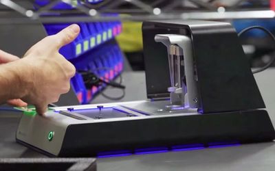
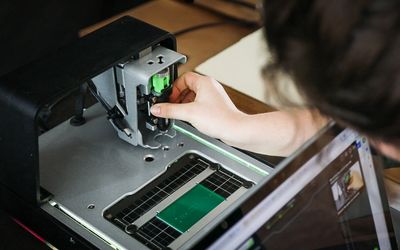
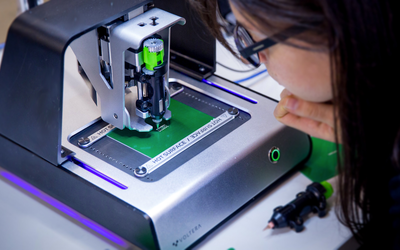
Voltera’s V-One benchtop printer is revolutionizing how electronics are developed with in-house, one-hour PCB prototyping.

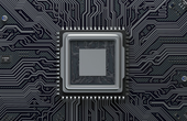
QFN packages are leadless and have short interconnects that reduce parasitic elements such as inductance and capacitance. How do they compare to other surface-mount ICs?
9 minutes read
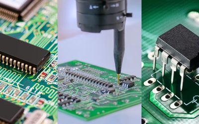
This detailed guide will cover the fundamentals of SMT vs SMD, and THT, exploring their working principle, advantages and disadvantages, comparative analysis, and choosing the right one for electronics assembly.
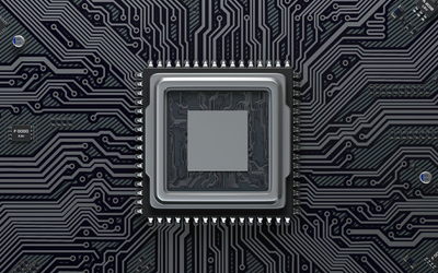
The Quad Flat No-leads (QFN) package is a type of surface-mount technology (SMT) in the electronics industry known for its compact size and high performance. This comprehensive guide explores its benefits (high performance), applications (mobile devices), and challenges (assembly, soldering).

Empowering AI-driven Industrial Automation with the OKdo DEBIX Model B in Extreme Conditions

Emerging technologies such as Voltera’s electronics printing solutions are making electronics design and prototyping more accessible and creating unprecedented opportunities for innovation.

The world of PCB connectors is diverse and expansive, catering to various applications in the field of electronics. In this article, we’ll dive and explore from the basics of board-to-board and wire-to-board connector types, to specialty connectors designed for specific use cases.
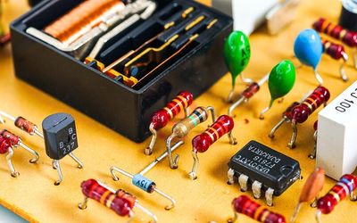
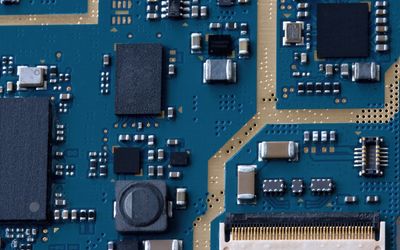
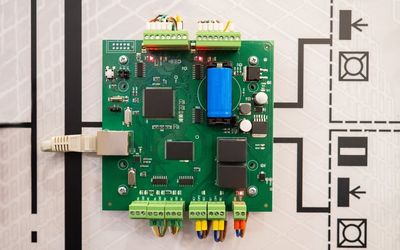
This guide provides an in-depth understanding of circuit board components, highlighting their basics, types, design process, and troubleshooting for various applications.
Chemical etching uses acidic chemicals to remove material and create an etched pattern on a metal surface. This article delves into the fundamental processes of chemical etching, its myriad applications, and nuanced techniques employed to achieve precision and perfection in the final product.
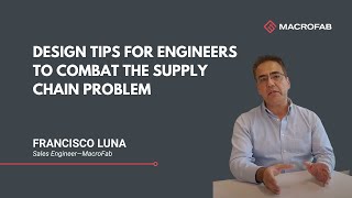
As Francisco Luna explains in this short video, the MacroFab technology platform provides superior visibility and flexibility to solve today's most common supply chain issues. Find out how you can speed up prototyping with MacroFab's technological platform prototyping and mitigate project risk.