Understanding PCB Mouse Bites: A Guide to Breakaway Tabs and V-Groove Techniques
Understanding the implementation, advantages drawbacks, and crucial design considerations for optimal circuit board separation and efficiency

11 Jan, 2024. 13 minutes read
PCB Panels are separated with pre-designed “Mouse Bites” for seamless and realiable operations
What is a PCB Mouse Bite?
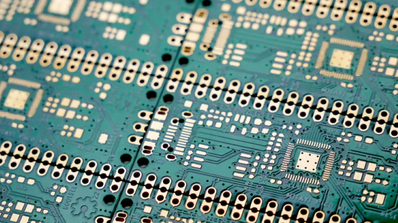
“PCB Mouse Bite” is a term used in the electronics manufacturing industry to describe a specific method of separating individual printed circuit boards (PCBs) from a larger panel during the manufacturing process. This method involves creating a series of small holes or perforations like postage stamps along the intended break line on the panel. Since these perforations resemble the marks left by a mouse bite, hence the name “PCB Mouse Bite”.
PCB Mouse Bite facilitates the safe and efficient separation of PCBs from the panel without causing damage to the circuitry or components on the board. This is particularly important in high-volume PCB manufacturing environments where hundreds or even thousands of PCBs need to be separated quickly and efficiently. It’s widely used in the electronics industry due to its simplicity, cost-effectiveness, and versatility.
The Advent of PCB Mouse Bites
The concept of PCB Mouse Bite has its roots in the early days of electronics manufacturing when there was a growing need for efficient and cost-effective methods of separating individual PCBs from a panel. As the electronics industry evolved and the complexity of PCB designs increased, so did the need for a reliable and damage-free method of PCB separation.
The initial concept of PCB Mouse Bite was quite time-consuming, labour-intensive, and heavily dependent on an individual’s skill.
Over time, the process of creating PCB Mouse Bites has been refined and automated with the introduction of specialized drilling machines and software that can accurately plot the location and size of the holes. This has significantly improved the speed and consistency of the process, making it a viable option for high-volume electronics manufacturing.
Based on the history and innovations in PCB Mouse Bite, it can be classified into two categories.
Early Stage Implementation
- PCB Mouse Bite was initially used in low-volume, high-cost electronics manufacturing to address concerns about PCB damage during separation.
- The process involved manual drilling of small holes along the intended break line, typically performed with a handheld drill or a simple drill press.
- Hole size and spacing were determined based on PCB thickness, material, and circuitry complexity, creating a weak point for controlled separation.
- It was a manual, slow, and error-prone process which was heavily reliant on the operator's skill, posing a risk of damage if holes were inaccurately drilled.
- PCBs with complex or dense circuitry were not suitable for this method due to the heightened risk of damage during the separation process.
Modern Day Implementation
- Modern PCB Mouse Bite has evolved into a highly automated process in today's electronics industry, utilizing computer-aided design (CAD) software and CNC drilling machines for precision.
- Specialized software is employed to plot hole locations and sizes on the PCB panel, enabling CNC drilling machines to achieve high precision and consistency in creating Mouse Bites.
- The process is adaptable, with adjustable hole sizes and spacing to meet specific PCB design and material requirements.
- 'Staggered' Mouse Bites, involving a staggered pattern of holes along the break line, provide a more controlled break point, particularly advantageous for PCBs with complex circuitry.
- 'Half-cut' Mouse Bites drill holes halfway through the PCB, leaving a thin layer for stability during manufacturing but allowing easy separation, resulting in cleaner edges.
Despite advancements, the fundamental principle of PCB Mouse Bite remains unchanged — creating a weak point for safe and efficient separation, reflecting its continued effectiveness and versatility in electronics manufacturing.
The Science Behind PCB Mouse Bite
The science behind PCB Mouse Bite follows the basic principles of mechanical engineering and materials science. The process involves creating a series of small holes or perforations along the intended break line on the PCB panel. These holes create a weak point in the panel, allowing it to be broken apart with minimal force.
Understandably, the effectiveness of PCB Mouse Bite largely depends on the holes' size, spacing, and pattern. These are the crucial parameters that must be carefully controlled to ensure a clean and predictable break point. Too large or too closely spaced holes can result in a rough or uneven edge on the separated PCBs, while too small or too widely spaced holes may not provide a sufficient weak point for easy separation.
Likewise, the PCB material also plays a crucial role in the effectiveness of PCB Mouse Bite. Different materials have different mechanical properties, such as strength, flexibility, and brittleness, which can affect the ease and quality of the separation.
Mechanical Aspects of PCB Mouse Bite
From a mechanical perspective, PCB Mouse Bite involves creating a controlled weak point in the PCB panel that allows for easy separation of individual PCBs. This is achieved by drilling a series of small holes along the intended break line on the panel.
- Size and Spacing - The holes need to be large enough to create a sufficient weak point in the panel, but not so large that they cause damage to the circuitry or components on the PCB. Similarly, the holes need to be spaced closely enough to ensure a clean and predictable break point, but not so closely that they weaken the structural integrity of the PCB.
- Hole Pattern - A staggered pattern, where the holes are offset from each other along the break line, can provide a more controlled and predictable break point compared to a straight-line pattern. This can be particularly beneficial for PCBs with complex or dense circuitry, where a clean and precise depanelization is critical.
- Material and Thickness - Different materials have different mechanical properties, such as strength and flexibility, which can affect the holes' size, spacing, and pattern. Similarly, the PCB's thickness can affect the holes' depth and the force required for separation.
Electrical Aspects of PCB Mouse Bite
The process of creating Mouse Bites can potentially affect the electrical properties of the PCB, such as impedance, signal integrity, and electromagnetic compatibility (EMC).
- Potential Circuitry Damage - The drilling of holes along the break line can create stress concentrations in the PCB material, which can lead to micro-cracks or delamination. These defects can, in turn, affect the electrical performance of the PCB by causing changes in impedance, signal attenuation, or crosstalk.
- Consideration of Electrical Parameters - The size and spacing of the holes should be carefully controlled to ensure that they do not interfere with the PCB's signal traces or ground planes. Additionally, the drilling process should be optimized to minimize the risk of damage to the PCB material, such as by using specialized drill bits or drilling techniques.
- Electromagnetic Emissions - PCB Mouse Bite can potentially increase electromagnetic emissions due to the presence of the holes. The holes can act as unintentional radiators, emitting electromagnetic energy that can interfere with other electronic devices or systems. To mitigate this issue, the design of the PCB should include appropriate shielding and grounding techniques, such as the use of ground planes or shielding layers.
- Overlapping Vias in a PCB - PCB Mouse Bites are often quite similar to PCB vias or circular solder pads. Therefore, it is essential to ensure proper demarcation of mouse bites to avoid confusion with the PCB vias. Otherwise, it can lead to faulty connections and damaged PCB performance.
Further Reading: Via in Pad PCB Design
Process of Implementing PCB Mouse Bite
The process of implementing PCB Mouse Bite involves several key steps, each of which requires careful planning and execution to ensure a successful outcome. Here is a breakdown for the process:
Design Phase
In the design phase, the location, size, and pattern of the Mouse Bites are determined based on the specific requirements of the PCB. This involves the use of computer-aided design (CAD) software to create a digital model of the PCB, including the Mouse Bites. At this step, there must be careful consideration of the mechanical and electrical properties of the PCB, and the intended method of separation.
Further Reading: How to Design a PCB Layout: A Comprehensive Guide
Drilling Phase
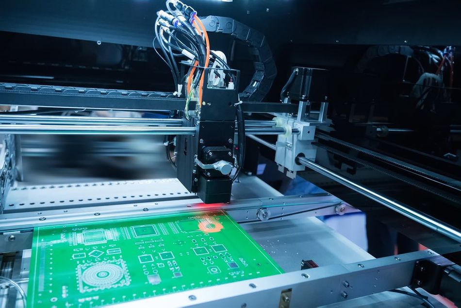
Drilling involves a CNC drilling machine to create the Mouse Bites on the PCB panel. The drilling machine is controlled by specialized software that uses the design data to plot the location and size of the holes accurately. While the process is generally automated, it must be carefully monitored to ensure the accuracy and consistency of the Mouse Bites, and to minimize the risk of damage to the PCB material.
Etching and PCB Assembly
After the drilling phase, the PCB panel undergoes the usual manufacturing processes, such as etching, soldering, and assembly. The Mouse Bites do not interfere with these processes, as they are designed to be robust enough to withstand the mechanical stresses involved.
PCB Separation
It is the final step in the process, where the individual PCBs are broken apart along the Mouse Bites. This is typically done manually, but can also be automated for high-volume manufacturing. The separation process needs to be carefully controlled to ensure a clean and damage-free break and to minimize the risk of damage to the circuitry or components on the PCB.
Design Considerations for PCB Mouse Bite
The design of PCB Mouse Bite is a critical factor in its success and effectiveness. The location, size, and pattern of the Mouse Bites need to be carefully considered to ensure a clean and predictable break point, while minimizing the risk of damage to the PCB.
Mouse Bite Location and Sizing
The location of the Mouse Bites is typically determined by the layout of the circuitry and components on the PCB. The Mouse Bites must be placed away from critical circuit elements and components to prevent damage during separation. They must also be evenly distributed along the break line to ensure a uniform break point.
While designing Mouse bites, most designers consider the following scheme:
- Hole size: 0.020 inch (0.5mm) diameter
- Spacing: 0.030 inches (0.76mm) apart from each other
However, the spacing and hole sizes can vary according to the PCB requirements. For instance, micro-sized or small PCBs with thinner material may require smaller holes as compared to thicker PCB materials.
PCB Thickness
Thicker PCBs or PCBs made of harder materials may require larger Mouse Bites to create a sufficient weak point. Conversely, thinner PCBs or PCBs made of softer materials may require smaller Mouse Bites to prevent excessive weakening of the panel.
Mouse Bite Pattern
The pattern of the Mouse Bites can also affect the performance of the depanelization process. A staggered pattern, where the Mouse Bites are offset from each other along the break line, can provide a more controlled and predictable break point. Conversely, a straight-line pattern may result in a more abrupt and less predictable break.
PCB Electrical Properties
In addition to mechanical considerations, there are also a few considerable electrical properties of the PCB, such as
- The Mouse Bites should not interfere with the signal traces or ground planes on the PCB,
- The drilling process should be optimized to minimize the risk of electrical issues, such as changes in impedance or increased electromagnetic emissions.
Advantages of Using PCB Mouse Bite
PCB Mouse Bite is a preferred method for separating individual PCBs from a panel. In addition to control and precision, here are some of its major benefits:
Clean Separation of PCBs
By creating a series of small holes along the intended break line, PCB Mouse Bite allows for a clean and predictable separation of the PCBs. This can be particularly beneficial for PCBs with complex or dense circuitry, where a clean and precise separation is critical.
Compatible with Automated Manufacturing Systems
PCB Mouse Bite is generally compatible with automated manufacturing processes. The drilling of the holes can be easily integrated into the PCB manufacturing process. So it allows automated separation of the PCBs for high-volume production. Hence, it can significantly increase the efficiency and productivity of the manufacturing process, and reduce the risk of human error.
Minimal Material Waste
PCB Mouse Bite also reduces material waste. Unlike other separation methods that require material removal along the break line, PCB Mouse Bite only requires the drilling of small holes. This not only reduces the amount of material waste but also minimizes the risk of damage to the PCB material.
Ensured Signal Integrity
From an electrical perspective, PCB Mouse Bite can also offer advantages in terms of maintaining the electrical integrity of the PCB. By carefully controlling the size, spacing, and pattern of the holes and optimizing the drilling process, it is possible to minimize the risk of electrical issues, such as changes in impedance or increased electromagnetic emissions. It’s a significant aspect, especially in multi-layered PCBs where internal wiring layers could be hidden.
Cost Effectivity
PCB Mouse Bite offer cost advantages. The drilling of the holes can be done using standard CNC drilling machines, without the need for specialized equipment or tools. Additionally, the process is scalable for high-volume production, which can lead to economies of scale and lower per-unit costs. Because of its wide-ranging set of advantages, Mouse Bites have become a standard separation mechanism for FR4 PCB materials.
Disadvantages and Challenges of Using PCB Mouse Bite
Despite its many advantages, PCB Mouse Bite also has certain disadvantages and challenges that need to be considered.
Possible Breakages
One of the main challenges is the need for precise control over the drilling process. The size, spacing, and pattern of the holes need to be accurately controlled to ensure a clean and predictable break point. Any inconsistencies in the drilling process can result in a rough or uneven board edge on the separated PCBs, or even damage to the PCB board material
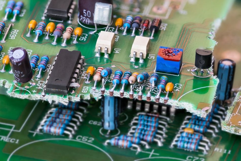 Fig 4: A damaged PCB due to uncontrolled or non-precise Mouse Bites
Stress on Electrical Connections
The drilling of the holes can create breakout stresses in the PCB material, which can lead to micro-cracks or delamination. These defects can affect the electrical performance of the PCB, causing changes in impedance, signal attenuation, or crosstalk. To mitigate these risks, the design and implementation of PCB Mouse Bite need to take into account the specific electrical requirements of the PCB.
A poorly designed PCB can incorporate incorrect mouse bite layouts. It especially happens due to excessive sharp turns and bendings. Eventually, such mouse bites can cause electrical signal disruptions and damage PCB performance.
Scalability
From a manufacturing perspective, PCB Mouse Bite can also present challenges in terms of scalability and efficiency. While the process can be automated for high-volume production, it can be time-consuming and costly for low-volume or prototype production. The drilling of the holes adds step to the manufacturing process, which can increase the production time and cost.
PCB Mouse Bite and Other PCB Breakaway Techniques
PCB Mouse Bite is one of several techniques used for separating individual PCBs from a panel. Other common techniques include V-grooving, and tab routing. Laser cutting may also be employed but it’s an uncommon practice. Each of these techniques has its own strengths and weaknesses, and the choice of technique depends on the specific requirements of the PCB.
V-Grooving
V-grooving involves cutting a V-shaped groove along the intended break line (also known as V-score) on both sides of the PCB panel. This creates a weak point that allows the PCBs to be easily broken apart. V-score offers a high degree of precision and control and can be easily automated for high-volume production. However, it requires specialized equipment and can result in a rough PCB edge on the separated PCBs. Additionally, the depth of the groove needs to be carefully controlled to prevent damage to the circuitry on the PCB.
 Fig 5: PCB panels featuring V-grooving separation
Tab Routing
Tab routing, on the other hand, involves cutting a series of breakout tabs along the break line using a CNC router. The tabs hold the PCBs in place during the manufacturing process and are removed after all the other processes are completed. Tab routing offers a high degree of flexibility, as the size and spacing of the breakout tabs can be easily adjusted to accommodate different PCB designs. However, it can be time-consuming and requires a high degree of precision to ensure a clean and damage-free break. Additionally, the routing process can generate a significant amount of dust and debris, which can contaminate the PCB and require additional cleaning.
Further Reading: PCB Panelization: Everything You Need to Know
Compared to these techniques, PCB Mouse Bite offers a good balance of precision, control, and efficiency. It does not require specialized equipment, and the drilling process can be easily integrated into the PCB manufacturing process. The size, spacing, and pattern of the Mouse Bites can be easily adjusted to accommodate different PCB designs, and the separation process is clean and predictable.
Conclusion
PCB Mouse Bite is a valuable technique for separating individual PCBs from a panel. It offers a balance of precision, control, and efficiency, and can be easily integrated into the PCB manufacturing process. However, it requires careful control over the drilling process to prevent damage to the PCB material, and may not be suitable for all types of PCBs. Despite these challenges, with careful design and implementation, PCB Mouse Bite can offer significant advantages in terms of productivity, cost-effectiveness, and electrical performance.
Frequently Asked Questions (FAQs)
What is PCB Mouse Bite?
PCB Mouse Bite is a technique used for separating individual PCBs from a panel. It involves drilling a series of small holes along the intended break line, creating a weak point that allows the PCBs to be easily broken apart.
How is PCB Mouse Bite implemented?
The implementation of PCB Mouse Bite involves several steps, including design, drilling, manufacturing, and separation. The design phase involves determining the location, size, and pattern of the Mouse Bites based on the specific requirements of the PCB. The drilling phase involves using a CNC drilling machine to create the Mouse Bites on the PCB panel. The manufacturing phase involves the usual processes such as etching, soldering, and assembly. The separation phase involves breaking apart the individual PCBs along the Mouse Bites.
What are the advantages of PCB Mouse Bite?
PCB Mouse Bite offers several advantages, including precision and control over the separation process, compatibility with automated manufacturing processes, minimal material waste, and potential cost savings. It can also help maintain the electrical integrity of the PCB by minimizing the risk of damage during separation.
What are the challenges of using PCB Mouse Bite?
The challenges of using PCB Mouse Bite include the need for precise control over the drilling process, potential for electrical issues due to stress concentrations in the PCB material, and scalability and efficiency challenges for low-volume or prototype production. It may also not be suitable for all types of PCBs, particularly those with very thin or fragile materials, or complex or high-density circuitry.
How does PCB Mouse Bite compare with other PCB breakaway techniques?
Compared to other techniques such as V-grooving and tab routing, PCB Mouse Bite offers a good balance of precision, control, and efficiency. It does not require specialized equipment, and the drilling process can be easily integrated into the PCB manufacturing process. However, it requires careful control over the drilling process to prevent damage to the PCB material, and may not be suitable for all types of PCBs.