




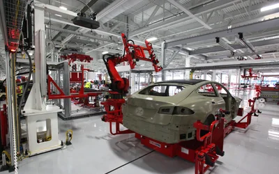
Robotic assembly lines have revolutionized production processes, enabling manufacturers to achieve high levels of efficiency, productivity, and quality.
Be the first to know.
Get our electronics weekly email digest.
Tagged with
electronics
ORGANIZATIONS. SHAPING THE INDUSTRY.
Latest Posts
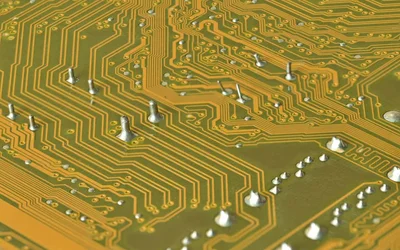
A cold solder joint is a defect caused by improper melting of solder to bond PCB electronic components. This defect can impact the functionality of a PCB assembly, and so must be carefully avoided.

Researchers have developed new technology that could usher in the "next-generation" of thinner, higher-resolution and more energy efficient screens and electronic devices.

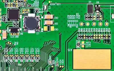
Testing PCBs involves using various methods and tools to ensure that all the individual elements of a PCB perform optimally, making up a high-quality PCB assembly. This article delves into the methods, procedures, and requirements of PCB testing.

EPFL researchers have come up with a new approach to electronics that involves engineering metastructures at the sub-wavelength scale. It could launch the next generation of ultra-fast devices for exchanging massive amounts of data, with applications in 6G communications and beyond.

3 minutes read


Without data, the IoT would be useless. The electromechanical and electronic sensors used to collect information are just as important to the IoT’s digital brains as sight, smell, hearing, and touch are to human organic ones.

3 minutes read


Article #7 of Innovations in Electric and Autonomous Vehicles Series: As electric vehicles (EVs) gain traction, challenges surrounding noise cancellation are dramatically changing, and the desire to reduce the weight of EVs is driving engineers toward active noise-cancellation solutions.


Article #5 of Innovations in Electric and Autonomous Vehicles Series: EV batteries and chargers evolve, and as traditional auto sales dropped, EV sales continued to rise over the past years. What will this mean for investors and consumers? Where is the tech taking us and what stands in the way?


Article #3 of Innovations in Electric and Autonomous Vehicles Series: 3GPP intends to use 5G in vehicle-to-everything (V2X) applications with significant advantages over current dedicated short-range communication or other cellular-V2X proposals.

11 minutes read

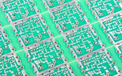
PCB Panelization is a PCB manufacturing technique. It involves the grouping of several small printed circuit boards to form a single array, which is known as a panel. Panelization is commonly employed in PCB manufacturing because it saves time and cost. This article discusses the conditions, design considerations, methods, types, and benefits of PCB panelization.
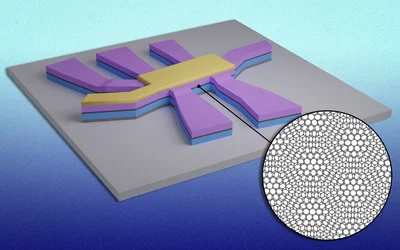
A quick electric pulse completely flips the material’s electronic properties, opening a route to ultrafast, brain-inspired, superconducting electronics.

Lead-free solders offer an environment-friendly alternative to toxic lead-based solders, which were dominant in the PCB manufacturing industry till the mid-2000s.

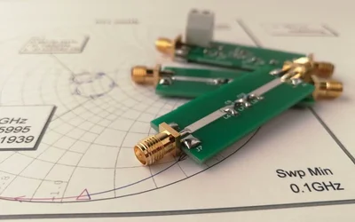
Controlled impedance in printed circuit boards involves the regulation of resistance exerted by signal traces. It is determined by characteristic factors of PCB fabrication, such as trace width and copper thickness. This article discusses controlled impedance and the essentials of its execution in PCB manufacturing.
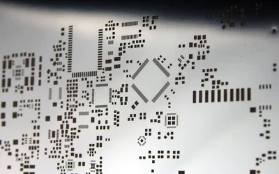
In this article, we will go over everything you need to know about PCB stencils.

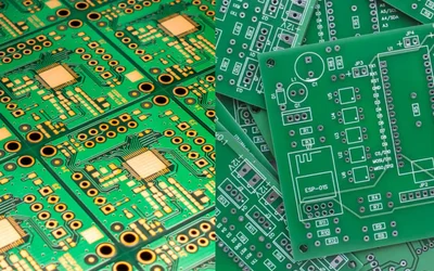
This article aims to provide a comparative analysis of HASL vs ENIG, providing valuable insights to aid in making informed decisions for PCB design and manufacturing.