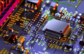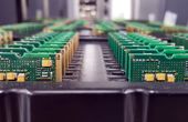


Electrical engineers must continually seek out new options and keep up with market changes. Take note of these six trends within the electronics industry.

5 minutes read
Tagged with
Electrical engineers must continually seek out new options and keep up with market changes. Take note of these six trends within the electronics industry.
5 minutes read
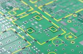
Vias go through two or more layers of PCBs to form an electrical connection. Making them right under the component’s pad saves space, reduces track inductance and simplifies design.
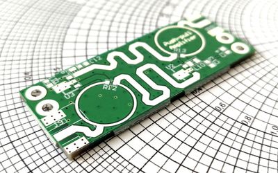
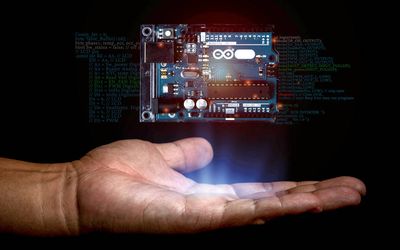
Show the world what you can create with cutting-edge single-board computer hardware.

5 minutes read
Advancements in power storage devices, Micro Electro Mechanical Systems (MEMS), Gallium Nitride (GaN) semiconductors, etc. are key to achieving carbon neutrality in various industries.

4 minutes read
The right programming method will be determined by the volume of your assembly run and the form factor of your device.
3 minutes read
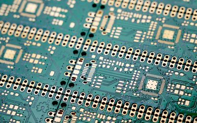
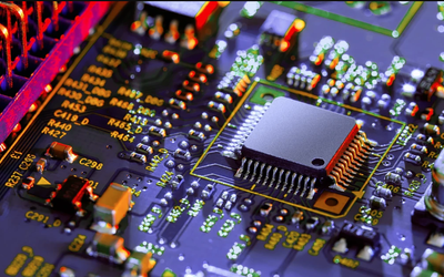
Printed Circuit Boards (PCBs) provide the foundation for the assembly of electronic components and enable the functionality of a wide range of devices. This article journeys through the requisite steps in the PCB manufacturing process, detailing the procedures involved in each.
It's difficult to protect every signal from noise intrusions, but this must be done to design an effective PCB assembly.
3 minutes read
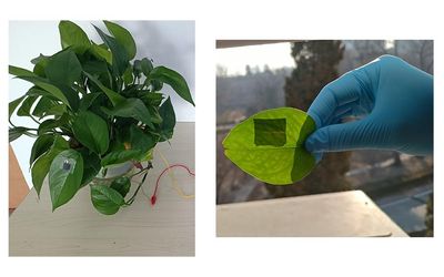
The popularity of wearable electronics has induced demand for their parts, including power sources such as triboelectric nanogenerators (TENGs). Such power sources must be both stretchy and high-performance, holding up under various deformation conditions over hours of use.

2 minutes read
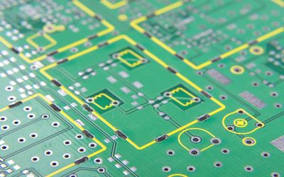
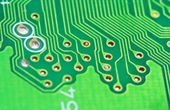
The silkscreen is a layer on the surface of a PCB that is used to identify a lot of information about the electronic printed circuit board.
PCBA design capabilities are crucial to the future of wearable technology. Wearables and PCBA design are inextricably linked since both have a significant influence on each other. As wearable devices become more popular, electronics designers and manufacturers are designing smaller, denser, and more flexible devices.
10 minutes read
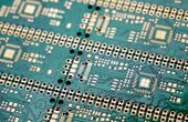
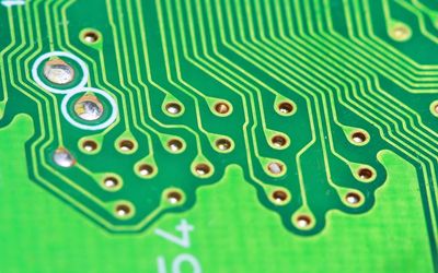
Vias are small holes in a PCB that enable electrical connections between different layers of the board. In the context of PCB design, via tenting refers to the process of covering the vias with a protective layer, typically a solder mask or dry film. This protective layer shields the vias from environmental factors, such as dust, moisture, and chemicals, which can lead to corrosion or short circuits. As PCB technology continues to advance, the importance of via tenting in maintaining the performance and reliability of complex, high-density interconnect (HDI) and flexible PCB designs cannot be overstated. This guide explores the art and science of via tenting, shedding light on its significance, techniques, and applications in modern PCB design and manufacturing.
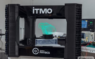
Researchers from ITMO University have come up with a new kind of wireless chargers – boxes with a uniformly distributed magnetic field inside them. Placing a device anywhere in the box will charge it, which makes the new technology stand out from its competitors, which can only ensure power transfer across short distances.

2 minutes read
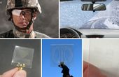
NANOWEB® is an extremely thin, transparent, conductive film that consists of an invisible, nanostructured metal mesh fabricated onto a glass or plastic surface. With its unrivaled transparency, conductivity, and flexibility, this patented functional film holds immense potential for both passive and powered use cases, with applications including electromagnetic interference shielding, antennas, 5G/6G redirection systems for elimination of dead spots, and deicing/defogging devices for vehicle windows and eyewear.
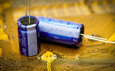
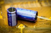
Capacitors store electrical energy, similar to batteries, and are used in many electronic devices. Due to their voltage-storing nature, handling them can be dangerous. This article outlines various techniques and safety measures to safely discharge capacitors.
What to know about the benefits of domestic prototyping
4 minutes read