How Switching Regulators Work: A Deep Dive for Power Engineers
This guide explores the theory behind switching regulators, compares the most common topologies, and details practical design considerations.

10 Feb, 2026. 18 minutes read
Key Takeaways
High efficiency through switching.
A switching regulator transfers energy by rapidly turning a transistor on and off within a closed-loop regulator circuit. Because the switch operates mostly in fully on or fully off states, power dissipation is minimized, and efficiencies above 90% are common when converting a higher-voltage power source to a lower voltage rail.
Multiple topologies serve different purposes.
Buck (step-down) converters reduce the input voltage to the desired output voltage, boost converters increase it, and buck‑boost converters can invert or adjust voltage levels. Flyback converters provide isolation and multiple outputs, while push-pull, half-bridge, and full-bridge converters extend the concept to higher-power applications.
Design is a balance of efficiency, noise, and size.
Factors such as inductor saturation, winding resistance, switching element losses, current limiting threshold, and diode forward voltage directly affect efficiency. Higher switching frequencies allow smaller magnetic and capacitive components but increase switching losses and electromagnetic interference.
Proper component selection and PCB layout are critical.
Selecting an inductor with sufficient saturation current, a low-resistance MOSFET, and a fast diode or synchronous rectifier can significantly improve performance. Careful PCB layout with short current loops helps reduce noise and electromagnetic radiation.
Emerging technologies are reshaping power conversion.
Gallium nitride (GaN) semiconductors are now widely used in low-voltage, high-efficiency designs. Integrated switching regulators with built-in FETs and digital control make systems easier to design and deliver higher power density.
Introduction
Power regulation is a fundamental requirement in electronic systems of all scales, from compact battery-powered devices to high-power industrial and automotive platforms. As digital logic, processors, and mixed-signal components continue to evolve, the need for stable, efficient, and precisely controlled power delivery has become increasingly critical. Poor power regulation can degrade performance, reduce reliability, and shorten system lifespan, making it a central concern in modern electronic design.
Early power-management solutions often favored simplicity over efficiency. Linear regulation, while easy to implement and inherently low in noise, becomes increasingly inefficient as voltage differences and load currents grow. Excess energy is dissipated as heat, leading to thermal challenges that limit scalability and impose additional design constraints. These limitations have become more pronounced as systems demand higher current at lower operating voltages.
At the same time, modern electronic products rarely rely on a single supply rail. Instead, they incorporate multiple voltage domains, each with distinct current, transient, and noise requirements. Generating these rails efficiently from a common input source requires power-conversion techniques that can adapt to varying conditions without incurring excessive power loss or occupying excessive board area. Consequently, switching regulators are the preferred solution in many contemporary power-electronics designs
This article examines switching regulators from a foundational and system-level perspective. It begins by exploring basic operating principles of switching regulators before progressing through converter topologies, control techniques, efficiency considerations, noise and electromagnetic interference challenges, and real-world applications. The goal is to provide a comprehensive technical understanding of switching regulators for power engineers, hardware engineers, and students who want to design DC/DC conversion circuits.
Fundamentals of Switching Regulators
What Is a Switching Regulator?
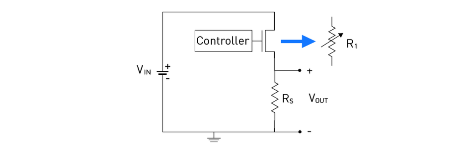
A switching regulator is a power-conversion circuit that maintains a regulated output voltage by rapidly switching an electronic device, most commonly a MOSFET, between on and off states. Instead of dissipating excess energy as heat, the regulator transfers energy in discrete packets through reactive components, allowing much higher efficiency than linear regulation.
Regulation is achieved by controlling parameters such as duty cycle, switching frequency, or peak current while continuously monitoring the output through a feedback loop. When the output voltage deviates from its target value due to changes in load or input voltage, the control circuitry adjusts the switching behavior to restore regulation.
Switching regulators operate at frequencies ranging from tens of kilohertz to several megahertz. Higher switching frequencies enable smaller passive components but increase switching losses and noise, requiring careful design trade-offs. Depending on topology and implementation, switching regulators can step voltage down, step it up, invert polarity, or provide galvanic isolation [1].
At a functional level, a switching regulator can be viewed as a feedback-controlled regulator circuit. Early and discrete implementations often used an operational amplifier (op amp) as an error amplifier to compare the output voltage with a reference. Modern integrated regulators embed this function internally, but the underlying principle remains the same.
Core Building Blocks of a Switching Regulator
Most switching regulators are composed of the following functional blocks:
Power Switching Element
A transistor, typically a MOSFET, alternates between conduction and cutoff states to control energy transfer. In low- to medium-power designs, the switch is often integrated into the regulator IC, while higher-power applications may use external devices.
Energy Storage Component
An inductor or transformer temporarily stores energy during each switching cycle and releases it to the load. The choice of magnetic component strongly affects efficiency, transient response, and physical size.
Rectification Path
A diode or synchronous MOSFET provides a current path when the main switch is off. Synchronous rectification reduces conduction losses and is commonly used in low-voltage, high-current designs.
Output Capacitor
The output capacitor smooths the pulsating current waveform, reduces voltage ripple, and supplies transient load currents.
Control and Feedback Circuitry
This circuitry senses the output voltage and adjusts switching behavior accordingly. It also implements protection functions such as overcurrent, overvoltage, and thermal shutdown.
Suggested Reading: Regulated vs. Unregulated Converters – When to Choose Which?
Switching Regulators Vs Linear Regulators
The fundamental difference between switching and linear regulators lies in how excess energy is handled. Linear regulators dissipate unused voltage as heat, making their efficiency proportional to the ratio of output voltage to input voltage. As voltage drop or load current increases, efficiency decreases, and thermal stress rises.
Switching regulators, by contrast, regulate voltage through controlled energy transfer rather than dissipation. As a result, efficiencies above 90% are achievable across a wide range of operating conditions. This advantage becomes especially significant in battery-powered, high-current, or thermally constrained systems.
The trade-off is increased complexity. Switching regulators introduce high-frequency noise, require careful component selection, and demand disciplined PCB layout to control electromagnetic interference and ensure loop stability. Despite these challenges, their efficiency, scalability, and flexibility make them the preferred solution in most modern electronic systems.
Switching Regulator Topologies
Several core topologies dominate DC/DC converter design. Each topology arranges the switch, inductor, and diode differently, which is typically illustrated using simplified schematics showing current flow during the on and off states of the switch. The table below summarises the main non‑isolated topologies and their properties.
Topology | Output relation (ideal) | Polarity | Key advantages | Typical applications |
Buck (step‑down) | Vout = D × Vin | Positive | Simple, efficient, continuous current to load | Point‑of‑load conversion, microcontroller supplies |
Boost (step‑up) | Vout = Vin/(1 − D) | Positive | Increases voltage, uses the same polarity | Battery‑powered devices needing higher voltage |
Buck‑Boost (inverting) | Vout = −D × Vin/(1 − D) | Negative | Output magnitude can be greater or less than Vin | Negative bias rails, bipolar supplies |
Flyback | Vout ≈ − (Ns/Np) × D × Vin/(1 − D) | Positive or negative | Provides isolation; multiple outputs | AC adapters, isolated bias supplies |
Push‑pull | Vout ≈ (D × Vin × Ns/Np)/2 | Positive | Two transistors share current, good for low Vin | Automotive power, low‑voltage high‑current supplies |
Half‑bridge | Vout ≈ (D × Vin × Ns/Np) | Positive | Efficient; good for AC inputs; moderate power | Offline power supplies |
Full‑bridge (H‑bridge) | Vout ≈ 2 × D × Vin × Ns/Np | Positive | Highest power handling; bidirectional | High‑power AC/DC converters, motor drives |
Non-Isolated Topologies
Non-isolated converters share a common electrical ground between the input and the output. They are widely used in low- to medium-power applications where galvanic isolation is not required
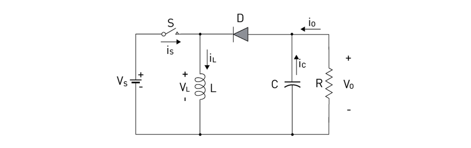
Buck (step‑down) Converter
The buck converter is the most common switching regulator. It lowers a DC input voltage to a lower voltage DC output with the same polarity. The buck converter uses a transistor that alternately connects and disconnects the input voltage to an inductor. When the switch turns on, the difference between the input and output voltages is forced across the inductor, causing the current to increase. Part of this current flows into the load, and part charges the output capacitor. When the switch turns off, the voltage across the inductor reverses to maintain current; the inductor current flows through the diode (or synchronous transistor) and the capacitor discharges into the load.
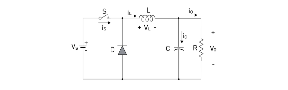
In continuous conduction mode, the average inductor current equals the load current, and the peak‑to‑peak ripple is typically kept below 20–30 % of the DC. The output voltage is given by Vout = D × Vin (ideal), though real circuits experience losses in the switch, diode, and inductor. The buck converter’s simplicity, high efficiency, and ability to maintain continuous current make it ideal for point‑of‑load regulation in digital systems. In multiphase buck regulators, multiple phases operate interleaved to reduce ripple and handle higher currents. Hysteretic, constant on‑time (COT), voltage‑mode, and current‑mode controllers each provide different transient response and noise characteristics.
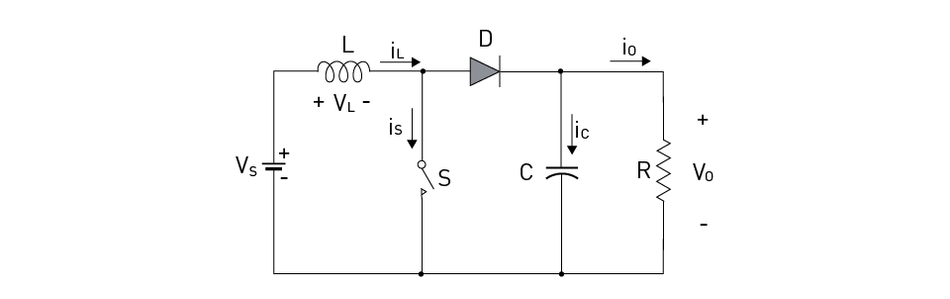
Boost (step‑up) Converter
A boost converter produces an output voltage higher than the input. When the switch is on, the input voltage is applied across the inductor, causing the current to ramp up. When the switch turns off, the decreasing inductor current forces the switch side of the inductor to swing positive, forward‑biasing the diode and charging the capacitor to a voltage higher than the input. The load draws current from the capacitor during the switch‑on time. An important design consideration is that the output load current is always less than the current rating of the switch because the output current is lower than the inductor current. Boost converters are common in battery‑powered systems that need to power sensors or amplifiers at higher voltages than the battery.
Buck‑Boost (inverting) Converter
The buck‑boost (or inverting) converter inverts the polarity of the input voltage and can provide an output magnitude either larger or smaller than the input. When the switch is on, the input voltage forces current through the inductor while the load current comes only from the output capacitor. When the switch turns off, the voltage across the inductor reverses, and the inductor current flows through the diode to the output capacitor and load. The negative output voltage equals −D/(1 − D) times the input voltage (ideal), though component losses alter this relation. Buck‑boost converters are useful for generating negative rails or when the input voltage can vary above and below the desired output. Non‑inverting buck‑boost topologies, such as SEPIC and ZETA, use two inductors or a coupled inductor to provide a positive output.
Flyback Converter
The flyback converter is the most versatile of the basic topologies. It uses a transformer instead of an inductor so that energy is stored in the transformer’s magnetic field during the on phase and delivered to the secondary winding during the off phase. The TI report notes that the flyback allows multiple outputs with different polarities and voltage levels by using multiple secondary windings. When the switch is on, the primary winding is energised, and the diode on the secondary is reverse‑biased, so the load receives current from the output capacitor. When the switch turns off, the primary current collapses and the voltage is reflected onto the secondary; the diode conducts, delivering energy to the output capacitor and load. Flyback converters provide galvanic isolation and are widely used in AC adapters, off‑line power supplies, and isolated gate drivers. Variants such as the active clamp flyback improve efficiency and reduce voltage stress.
Suggested Reading: DC to AC Inverter Circuits – Theory, Design and Practical Implementation
Push‑pull, Half‑bridge, and Full‑bridge
When higher power levels are required, designers move beyond single‑switch topologies. Push‑pull converters use two transistors to alternately drive opposite halves of a transformer primary. This configuration is efficient for low‑voltage inputs and supports higher power by splitting the input current.
Half‑bridge converters use two transistors and a split capacitor network to generate a quasi‑square waveform on the transformer; they are common in off‑line power supplies. Full‑bridge converters (also called H‑bridge) use four transistors to drive the transformer in both directions, delivering the highest power capability. Survey data indicate that full‑bridge converters are popular; nearly half of the respondents reported designing them. Resonant converters (LLC) and multi‑level converters extend these topologies with soft switching (zero‑voltage or zero‑current switching) to achieve high efficiency at high frequencies.
Design Considerations and Efficiency
Achieving high efficiency is a central goal when designing a switching regulator. Efficiency (η) is defined as the ratio of output power to input power. Efficiency improvement is important because every watt wasted manifests as heat and decreases battery life. Several factors influence the efficiency of a switching regulator:
Inductor Selection
An inductor’s saturation current must exceed the peak inductor current. If the inductor saturates, its inductance collapses, and the current rises rapidly, causing high losses or damage. Circuit Cellar’s experiments showed that using a toroidal 330 μH inductor with high saturation current yielded ~72 % efficiency, whereas a physically smaller inductor suffered lower efficiency due to higher series resistance [2]. Designers should choose inductors with low direct current resistance (DCR) to reduce conduction losses. Ferrite cores are preferred at high frequencies because they have low core losses. Shielded inductors reduce EMI but may have higher DCR.
The inductance value determines the current ripple; too small an inductance increases ripple and diode conduction losses, while too large an inductance increases size and cost. A common design target is to keep the peak‑to‑peak ripple current between 20 % and 30 % of the load current.
Switch (transistor) Selection
The switching element can be a bipolar junction transistor (BJT), MOSFET, or, increasingly, a wide‑bandgap device such as GaN. The on‑state resistance (R_DS(on)) or saturation voltage determines conduction losses. Bipolar transistors operated in saturation have a finite voltage drop, and their switching speed depends on stored charge; using a MOSFET reduces these losses. However, MOSFETs have gate charge that must be driven quickly; if the gate drive is weak, switching transitions become slower, and losses increase. Wide‑bandgap MOSFETs (GaN, SiC) offer lower R_DS(on), lower gate charge, and higher switching speeds than silicon MOSFETs, enabling higher efficiency and higher switching frequency.
Proper gate drive is critical. A gate resistor balances switching speed and ringing; high gate resistances slow down switching and reduce EMI, while low resistances speed up switching but can cause overshoot. Driver ICs must supply sufficient peak current to charge and discharge the gate capacitance quickly. High‑side gate drivers or bootstrap circuits enable N‑channel MOSFETs to be used for both high‑side and low‑side positions.
Diode or Synchronous Rectifier
In a simple converter, the diode conducts during the off phase. The forward voltage drop directly reduces efficiency. Circuit Cellar compared standard diodes with Schottky diodes; a 1N4001 (≈0.8 V drop) dissipated considerable power, while a Schottky diode with ≈0.4 V drop improved efficiency. At high currents, the conduction loss (I × V_F) becomes significant. Synchronous rectifiers replace the diode with a MOSFET that is actively driven to conduct during the off phase. Because the MOSFET’s R_DS(on) can be milliohms, conduction losses are much lower. Synchronous converters must implement dead time between switching transitions to prevent shoot‑through. Many modern buck regulators integrate the high and low‑side MOSFETs and handle synchronous control internally.
Switching Losses and Drive Circuitry
When a transistor switches between off and on, there is a brief period where both the voltage across and the current through the device are non‑zero. The instantaneous power (P = V × I) during this transition results in switching losses. These losses increase with switching frequency and gate charge. A strong gate driver reduces transition time and lowers switching loss but increases gate‑drive power consumption. Minimising parasitic inductance and capacitance in the PCB layout reduces voltage overshoot and ringing, which can also cause power loss.
Output Capacitor Selection
The output capacitor supplies load current during the off phase and filters the voltage ripple. Its capacitance value and equivalent series resistance (ESR) determine the output ripple voltage. Low‑ESR ceramic capacitors reduce ripple but may cause control‑loop instability in some regulators. Electrolytic or tantalum capacitors provide high capacitance but have higher ESR. A combination of different capacitor types often yields the best performance. Designers should also consider the capacitor’s voltage rating, temperature coefficient, and ageing.
Efficiency Estimation
Efficiency can be estimated by summing individual losses: conduction losses in the inductor and MOSFET, diode or synchronous MOSFET conduction losses, switching losses, core losses in the magnetic components, capacitor ESR losses, and control circuitry consumption. For accurate estimation, designers can use the manufacturer’s models, simulation tools, and efficiency curves provided in datasheets. Modern integrated regulators often exceed 90 % efficiency thanks to synchronous rectification, optimized gate drivers, and integrated power stages.
Managing Noise, Ripple, and EMI
Switching converters introduces ripple and noise on their outputs. Understanding the sources of noise and implementing mitigation strategies is essential for sensitive digital circuits.
Switching Ripple
The primary noise component is switching ripple—a periodic voltage ripple at the switching frequency and its harmonics. The ripple amplitude depends on the duty cycle and the inductor–capacitor (LC) filter transfer function. The fundamental component dominates when the duty cycle is around 50 %. Increasing the output capacitor or inductor reduces ripple amplitude, as does increasing the switching frequency. A post‑filter (LC or RC) can further attenuate ripple if the converter’s control loop remains stable.
Wideband Noise and Spikes
Wideband noise results from random amplitude variations due to semiconductor processes, reference noise, and control loop noise. Analog Devices notes that wideband noise is typically in the 10 Hz to 1 MHz range and is much smaller in amplitude than switching ripple [3]. However, if ripple is filtered by a post‑filter, wideband noise may dominate. High‑frequency spikes occur when the switch turns on and off; they are caused by parasitic inductances and capacitances and can be reduced by proper snubbing networks and layout.
Power Supply Rejection and Filters
The power supply rejection ratio (PSRR) of downstream circuits determines how much noise is tolerated. In noise‑sensitive applications, a low‑noise LDO can be placed after the switching regulator to filter out ripple and wideband noise. This cascaded approach sacrifices some efficiency but provides a clean supply for analog circuits. Alternatively, designing a low‑noise switching regulator—using current‑mode control, optimizing compensation networks, and adding post‑filters—can achieve performance comparable to LDOs.
EMI and Layout
Switching regulators can radiate electromagnetic interference due to high di/dt and dv/dt transitions. Emerald Technologies’ layout article stresses that switchers work by rapidly turning the power switch on and off; during the ON state, the switch is saturated with negligible voltage drop, and during the OFF state, it blocks current with negligible leakage, leading to very efficient conversion. However, these fast transitions create current loops that can act as antennas. The article emphasises that switching supplies offer advantages in miniaturization and power efficiency, but require careful layout and filtering to control EMI [4]. Key layout practices include:
Keep high‑di/dt loops (between the switch, inductor, and input capacitor) as short as possible and route them over a solid ground plane.
Place the output capacitor close to the load and return currents to ground via a low‑impedance path.
Separate noisy switching nodes from sensitive analog or digital circuitry.
Use continuous ground planes and avoid split planes that force current to travel long paths.
Add input and output filtering (ferrite beads, LC filters) where necessary.
Observing these guidelines reduces conducted and radiated EMI and improves reliability.
Control Methods & Modes
The control scheme determines how the duty cycle is modulated to maintain a constant output voltage under varying input and load conditions. Common methods include:
Voltage‑mode control. The controller compares the output voltage to a reference and adjusts the duty cycle accordingly. Voltage‑mode control is simple and provides good load regulation, but requires compensation to achieve stability over different input voltages and loads. Transient response can be slower because the controller reacts to output voltage changes.
Current‑mode control. The controller monitors the inductor current in addition to the output voltage. This inner current loop provides inherent over‑current protection and simplifies compensation. Current‑mode converters respond quickly to load transients and are widely used in modern buck and boost regulators.
Hysteretic (bang‑bang) control. Also called ripple‑mode or constant on‑time control, hysteretic regulators toggle the switch when the output voltage crosses upper and lower thresholds. They respond extremely quickly to load changes and do not require compensation, but their switching frequency varies with load and input, which can complicate EMI filtering.
Fixed‑frequency controllers with constant on‑time (COT). COT controllers set a fixed on‑time and adjust off‑time to regulate output voltage. They maintain nearly constant switching frequency across line and load variations, improving efficiency and simplifying filter design. Many modern TI buck regulators use COT architectures to achieve fast transient response.
Digital control. Digital controllers use microcontrollers or DSPs to sample the output and compute the duty cycle adjustments algorithmically. They enable advanced features such as adaptive voltage scaling, programmable soft start, telemetry, and fault reporting. Digital control is common in server power supplies and high‑current point‑of‑load regulators and is supported by standards such as PMBus and SVID. An example is TI’s TPS544B27W synchronous buck converter, which offers PMBus and SVID interfaces and 20 A output current.
PWM vs. PFM Operation
Pulse-Width Modulation (PWM)
In PWM, the switching frequency is fixed, and the duty cycle is varied to maintain regulation. PWM provides predictable frequency characteristics, simplifying filter design, and is well-suited for medium- to high-load applications where efficiency is less sensitive to light-load conditions.
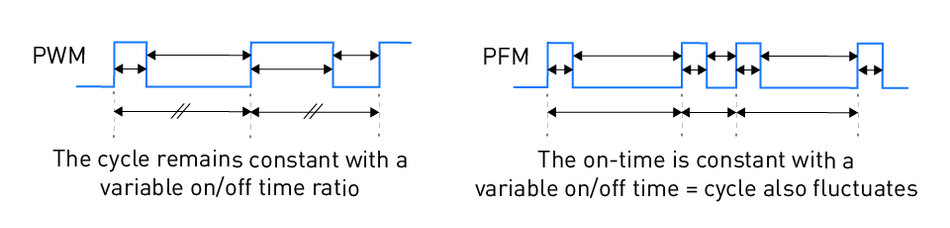
Pulse-Frequency Modulation (PFM)
PFM varies the switching frequency while maintaining a fixed pulse width to control output voltage. This technique improves light-load efficiency by reducing switching losses but can generate variable-frequency noise and may complicate EMI filtering.
Hybrid Approaches
Many modern regulators use hybrid control methods that switch between PWM and PFM depending on load conditions, optimizing both efficiency and noise performance across a wide operating range.
Conduction Modes
Continuous Conduction Mode (CCM)
In CCM, the inductor current never falls to zero during the switching cycle. CCM provides low ripple and predictable dynamics but may result in higher switching losses at light loads.
Discontinuous Conduction Mode (DCM)
In DCM, the inductor current falls to zero before the end of each cycle. DCM can improve efficiency at light loads and reduce inductor size, but increases peak currents and requires careful control-loop design.
Boundary/Critical Conduction Mode
The boundary conduction mode operates at the transition between CCM and DCM. It offers a compromise between efficiency, component stress, and transient response, providing high light-load efficiency while maintaining stable operation.
Applications of Switching Regulators
Switching regulators are used in virtually every sector of modern electronics, from consumer devices to industrial systems. Their efficiency, flexibility, and ability to handle varying input and output conditions make them ideal for diverse applications.
Consumer Electronics
In smartphones, laptops, tablets, and wearable devices, switching regulators provide multiple low-voltage rails required by processors, memory, sensors, and display drivers. High efficiency is essential to maximize battery life while minimizing heat in compact enclosures.
Industrial Systems
Industrial automation equipment, programmable logic controllers (PLCs), and motor drives rely on switching regulators to deliver precise voltages under high-load and noisy conditions. High efficiency reduces energy costs and ensures reliable operation in thermally demanding environments.
Automotive Electronics
Modern vehicles incorporate dozens of electronic subsystems, from infotainment and advanced driver-assistance systems (ADAS) to electric powertrains. Switching regulators provide regulated voltages from 12 V or 48 V battery systems, while handling load transients, wide temperature ranges, and stringent automotive standards.
Telecom and Networking
Servers, routers, base stations, and networking switches require high-density, high-efficiency power conversion. Switching regulators deliver stable voltages for processors, FPGAs, and memory modules while minimizing power losses and thermal management challenges.
IoT and Low-Power Embedded Systems
Battery-powered IoT devices and embedded sensors often operate at milliwatt power levels. Switching regulators extend battery life by operating efficiently over wide input voltage ranges and supporting energy-harvesting systems.
Emerging Technologies and Trends
Wide‑bandgap Semiconductors
Industry surveys reveal a strong shift toward wide‑bandgap semiconductors in power converters. Power Electronics News’ 2025 survey report notes a dramatic surge in wide-bandgap adoption, with low-voltage GaN usage increasing sixfold year-over-year [5]. GaN transistors offer several advantages over silicon MOSFETs: lower R_DS(on), lower gate charge, faster switching speed, and improved thermal performance. These properties enable higher switching frequencies, higher efficiency, and smaller magnetics. GaN devices are increasingly available in half‑bridge modules and integrated converter ICs. Silicon carbide (SiC) devices, although used more in high‑voltage applications, also provide improved efficiency and high‑temperature capability.
Integrated and Digital Regulators
Integrated regulators with onboard FETs simplify PCB design and reduce component count. Texas Instruments highlights that its AC/DC and DC/DC converters integrate one or more FETs and offer a balance of flexibility and ease of use across many topologies. Many new products combine synchronous MOSFETs, controllers, drivers, and compensation networks into a single package, often in small QFN footprints. Some devices also integrate magnetics in so‑called “power modules” to provide a complete DC/DC converter requiring only input and output capacitors.
Digital control is growing, especially in server and high‑current point‑of‑load regulators. Digital converters support programmable output voltage, dynamic voltage scaling, telemetry, and fault logging via PMBus or SVID. They can implement nonlinear control algorithms for better transient response and adaptively adjust switching frequency and dead time. Integrated voltage regulator (IVR) technology places the regulator directly beneath or on the processor package, reducing voltage droop and improving transient response.
Advanced Topologies
Zero‑voltage switching (ZVS) and zero‑current switching (ZCS) are techniques that reduce switching losses by ensuring that the voltage or current across the switch is zero at the moment of transition. Resonant topologies such as LLC converters use these techniques to achieve high efficiency at high frequencies. Multiphase and interleaved converters distribute the load current across multiple phases, reducing ripple and improving transient response. Multi-level converters combine several lower-voltage stages to produce high voltage with reduced switching losses and harmonic distortion. These advanced topologies are increasingly used in electric vehicles, renewable energy inverters, and high‑density server power supplies.
Conclusion
Switching regulators are indispensable in modern electronics. They convert voltages efficiently by storing and releasing energy rather than dissipating it as heat. Fundamental topologies—buck, boost, buck‑boost, and flyback—form the building blocks of countless power supplies, while more complex push‑pull, half‑bridge, and full‑bridge converters extend the power range. Key design considerations include selecting the right topology, choosing components with suitable ratings and low losses, controlling noise and EMI through careful layout, and deciding on an appropriate control method. Emerging technologies such as GaN semiconductors, integrated regulators and digital control promise higher efficiency, greater power density and improved programmability. Whether you are powering a microcontroller in a wearable device or designing a kilowatt‑level server power module, understanding switching regulators will enable you to build robust and efficient systems.
Frequently asked questions (FAQ)
1. What is the difference between a switching regulator and a linear regulator?
A linear regulator uses a pass transistor operating in its linear region to drop the input voltage to the desired output, dissipating the excess voltage as heat. It provides low noise but is inefficient when the input voltage is much higher than the output.
A switching regulator rapidly switches a transistor on and off, using an inductor or transformer to temporarily store energy and deliver it to the output at a different voltage. Because the switch operates either fully on or fully off, switching regulators achieve much higher efficiency.
2. How do I choose between buck, boost and buck‑boost topologies?
If your input voltage is always higher than the desired output, a buck (step‑down) converter is appropriate. If the input is lower and you need a higher output, use a boost converter. When the input can be above or below the required output or you need a negative output, choose a buck‑boost or related topology (e.g., SEPIC or ZETA). Flyback converters are used when isolation or multiple outputs are required.
3. What factors affect switching regulator efficiency?
Efficiency is influenced by conduction losses in the inductor and switch (due to DCR and R_DS(on)), diode forward voltage or synchronous MOSFET conduction loss, switching losses during transitions, core losses in magnetic components, capacitor ESR, and control circuitry consumption. Proper component selection, adequate gate drive, synchronous rectification, and optimal switching frequency help maximise efficiency.
4. What is ripple, and how can it be reduced?
Ripple is a periodic variation in the output voltage at the switching frequency and its harmonics. It arises from the inductor and capacitor discharging and charging. Ripple amplitude can be reduced by increasing the inductance or capacitance, using capacitors with lower ESR, operating at a higher switching frequency, and adding a post‑filter. For noise‑sensitive circuits, follow the switching regulator with a low‑noise linear regulator.
5. Why are GaN devices important for switching regulators?
Gallium nitride transistors have lower on‑resistance, lower gate charge, and higher switching speed than silicon MOSFETs. These properties reduce conduction and switching losses, enabling higher efficiency and higher switching frequencies. Surveys show that low‑voltage GaN usage is increasing rapidly in power electronics designs.
6. How does switching frequency impact design?
Higher switching frequency allows smaller inductors and capacitors, reducing solution size. However, switching losses increase with frequency, and EMI becomes harder to control. Designers must balance component size, efficiency, cost, and EMI when selecting frequency.
7. What are the key PCB layout guidelines for switching regulators?
Keep high‑current loops small and close to the ground plane, place input and output capacitors near the converter IC, separate noisy nodes from sensitive circuitry, use wide traces or copper pours for power paths, and provide adequate thermal paths. Following these practices reduces EMI and improves reliability.
References
[1] Texas Instruments, “Switching Regulator Fundamentals,” Application Report.
Available: https://www.ti.com/lit/an/snva555/snva555.pdf
[2] J. Slone, “Switching Regulator Efficiency,” Circuit Cellar, no. 259, pp. 22–29, 2012.
Available: Link
[3] Analog Devices, “Comprehensively Understand and Analyze Switching Regulator Noise,” Technical Article.
Available: Link
[4] Emerald Technologies, “Switching Power Supply PCB Layout Considerations,” Blog Article.
Available: Link
[5] Power Electronics News, “2025 Power Converter Technology Survey Report,” 2025.
Available: Link
in this article
1. Key Takeaways2. Introduction3. Fundamentals of Switching Regulators4. Switching Regulator Topologies5. Design Considerations and Efficiency6. Managing Noise, Ripple, and EMI7. Control Methods & Modes8. Applications of Switching Regulators9. Emerging Technologies and Trends10. Conclusion11. Frequently asked questions (FAQ)12. References