Fully Depleted Silicon on Insulator (FDSOI) Theory, Design and Applications for Modern Engineers
A comprehensive overview of fully depleted silicon on insulator technology, covering device physics, process nodes and practical design approaches to help digital and hardware engineers leverage FDSOI for low power, high performance, and RF/mm wave applications.

04 Nov, 2025. 11 minutes read
Key takeaways
FDSOI uses ultra-thin buried oxide and a very thin silicon channel (UTBB) to create a fully depleted device that. does not require channel doping. It offers improved electrostatic control, lower leakages and parasitic capacitances, and avoids random dopant fluctuations.
FDSOI allows designers to dynamically tune the threshold voltage through forward and reverse body bias, which enables performance boosting or power reduction without changing supply voltage.
Because of its planar structure, FDSOI requires fewer process steps and masks than FinFETs. Many FDOIS platforms deliver FinFET like performance at a lower cost and smaller die area, requiring fewer masks. Hence, it’s a cost-effective option against its counterparts.
FDSOI offers low leakage, wide body‑bias range and excellent analog characteristics, which makes it a viable option for microcontrollers and FPGAs, ultra‑low‑power IoT chips, high‑speed RF transceivers and even 77–81 GHz automotive radar systems. It can operate reliably at high temperature (up to 300 °C) thanks to near‑ideal sub‑threshold swing and reduced junction area.
FDSOI has a growing ecosystem as more than 350 million FDSOI chips have shipped, generating over US$4.5 billion in revenue. STMicroelectronics, GlobalFoundries, and Samsung are now making 28nm, 22nm, and 18nm nodes. In the future, the FDSOI market will extend to 10nm and beyond, integrating eMRAM, RF and 3D stacked designs.
Introduction
The trade-off between power and performance is a major challenge in the semiconductor scaling sector. Modern digital industries like Edge artificial intelligence, automotive electronics, and the Internet of Things (IoT) demand chips that deliver high compute density with extremely low energy per operation. But the traditional bulk CMOS struggles to suppress leakage as gate lengths shrink, while multi‑gate FinFETs—though powerful—introduce complexity and cost.
However, thanks to a planar alternative, fully depleted silicon‑on‑insulator (FDSOI), there is a compelling solution in the offering. By placing an ultra‑thin buried oxide (BOX) under a very thin silicon channel (the ultra‑thin body), FDSOI devices become fully depleted without channel doping. This simple structural change yields profound improvements in electrostatics, enabling aggressive scaling with low leakage, reduced variability, and new design freedoms through body‑biasing. This article provides an in‑depth technical exploration of FDSOI for digital design engineers, hardware designers, and electronics engineering students. Beginning with the physics of the UTBB FDSOI transistor and its advantages over bulk CMOS and FinFETs.
Suggested Reading: Understanding Transistors: What They Are and How They Work
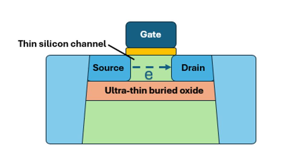
Fundamentals of FDSOI Ultra‑thin body and buried oxide structure
Conventional MOSFETs use thick silicon substrate, so the channel region is part of the bulk. By contrast, FDSOI transistors are fabricated on silicon‑on‑insulator wafers where a thin silicon film (typically 7–12 nm) sits atop a buried oxide of 20–25 nm.
In the Ultra‑Thin Body & Buried Oxide (UTBB) configuration, the channel thickness is so small that mobile carriers are fully depleted when the device turns off, eliminating the need for channel doping.
Benefits of the UTBB Structure
Improved electrostatic control: The buried oxide electrically isolates the body, reducing parasitic capacitance and improving gate control over the channel. The sub‑threshold slope and drain‑induced barrier lowering (DIBL) are significantly better than in bulk devices.
Reduced variability: Without channel doping, there are no random dopant fluctuations; this leads to a tighter threshold voltage (V<sub>t</sub>) distribution and better matching.
Lower leakage and parasitic capacitance: The buried oxide suppresses junction leakage and reduces body charging, enhancing retention in SRAMs and analog circuits.
Simplified process flow: FDSOI is planar and uses fewer masks and process steps than FinFET technologies. GlobalFoundries notes that its 22 nm FDSOI node (22FDX) results in 20 % smaller die area and about 10 % fewer masks compared with 28 nm processes.
Device Physics and Electrostatics
A fully depleted channel means that the depleted region spans the entire silicon thickness. Consequently, the sub‑threshold swing approaches the thermal limit (∼60 mV/decade at room temperature).
Moreover, studies on high‑temperature FDSOI devices show near‑ideal sub‑threshold swings of 65–70 mV/decade and leakage currents orders of magnitude lower than bulk devices even at 300 °C. Additionally, the buried oxide reduces the capacitance between source/drain and body, leading to faster switching and lower dynamic power.
Because FDSOI devices do not require channel doping, the threshold voltage is controlled by the gate work function and the channel thickness. This eliminates random dopant fluctuations, enabling precise Vt tuning via body biasing.
The ultra‑thin silicon film also facilitates short‑channel scaling. In a 28 nm UTBB FDSOI process, the channel length can be scaled down to 24 nm, compared with ~28 nm for bulk CMOS.
Comparing FDSOI with Other Technologies
Bulk CMOS and FinFETs
Bulk CMOS remains dominant at older nodes but suffers from increasing leakage, variability, and latch‑up when scaled below 28 nm. FDSOI’s buried oxide mitigates these issues, providing better electrostatic control and latch‑up immunity.
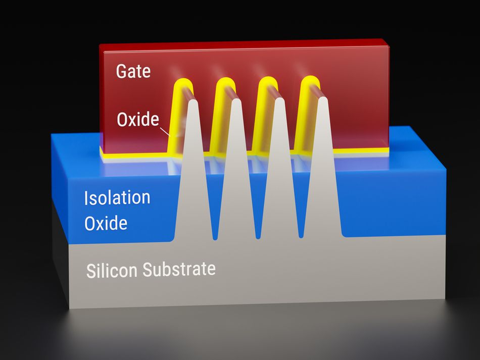
FinFETs use a 3‑D tri‑gate structure that wraps the gate around a fin. FinFETs offer excellent control at very small dimensions (7 nm and below), but require complex manufacturing, new design rules, and higher cost. They also have limited body‑bias capability and suffer from self‑heating due to the tall fin structure.
Because FDSOI is planar, it requires fewer lithography steps and masks and can deliver FinFET‑like performance at lower cost. However, FDSOI wafers are more expensive because the buried oxide and thin silicon layers are engineered, and there is some self‑heating due to the oxide’s poor thermal conductivity.
Suggested Reading: Silicon Wafers: Production, Properties and Application
Partially Depleted SOI (PD‑SOI)
Early PD‑SOI technologies (around 2003–2008) used thicker silicon bodies (>50 nm). These devices were easier to manufacture but left part of the body undepopulated, leading to floating body effects and dynamic threshold variations.
FD‑SOI solves these issues by using an ultra‑thin body that is completely depleted. PD‑SOI remains relevant in high‑voltage or high‑performance analog designs, but FDSOI is superior for low‑power logic and RF.
Summary of Advantages and Challenges
Below is a concise comparison of FDSOI, bulk CMOS, and FinFET technologies. The table uses keywords and phrases rather than long sentences to improve readability.
Technology | Key characteristics | Advantages | Challenges |
FDSOI | Planar transistor on ultra‑thin buried oxide; ultra‑thin silicon channel; no channel doping |
|
|
Bulk CMOS | Thick silicon substrate; heavily doped wells and channels |
|
|
FinFET | 3‑D fin structure; gate surrounds fin; multi‑gate control |
|
|
PD‑SOI | Thicker silicon body with partial depletion |
|
|
Further Reading: Silicon Semiconductor: A Comprehensive Guide to Silicon and its Use in Semiconductor Technology
Manufacturing and Process Nodes
28 nm FDSOI and the Origins
FDSOI traces its roots back to research at UC Berkeley and Leti in the early 2000s, with commercial support from Soitec (substrate supplier), CEA‑Leti (research), STMicroelectronics, and Renesas.
The first 28 nm FDSOI processes entered volume production around 2012–2014.
STMicroelectronics built a UTBB FDSOI platform using a 7 nm silicon film and 25 nm buried oxide, enabling channel lengths down to 24 nm.
Samsung licensed this technology and announced a 28FDS platform for mobile and IoT SoCs in 2014.
22 nm FDSOI (22FDX)
GlobalFoundries (GF) pioneered a 22 nm FDSOI platform known as 22FDX. In 2015, GF announced that 22FDX achieves FinFET‑like performance at 20% lower power, with 0.4V operation, 20% smaller die area, and 10 % fewer masks relative to 28 nm FDSOI.
The platform eliminates many immersion lithography steps which resulted in a lowered cost. It also integrates embedded MRAM (eMRAM) and supports variants optimized for ultra‑low power (22FDX‑ulp), high performance (22FDX‑uhp), ultra‑low leakage (22FDX‑ull), and RF applications (22FDX‑rfa).
By 2020, GF had shipped over 350 million 22FDX chips, generating more than US$4.5 billion in revenue. GF’s body‑bias ecosystem provides foundation IP, adaptive power management, and design automation tools to exploit dynamic threshold control.
Emerging Nodes: 18 nm and Beyond
Samsung and STMicroelectronics continue to push FDSOI to 18 nm (18FDS) and beyond. Samsung’s presentations highlight 18FDS+ as an enhanced 18 nm FDSOI node that further improves RF characteristics and reliability, offering around 10 % performance improvement and 30 % power reduction compared with 28 nm.
Public articles mention plans for mass production around 2025, targeting mm‑wave radar and low‑power AI applications. Research roadmaps from European projects (e.g., FAMES) envision UTBB FDSOI scaling toward 10 nm nodes with improved electron mobility and integration of embedded non‑volatile memories (eMRAM, RRAM) and 3‑D sequential stacking.
Wafer Engineering and Costs
FDSOI depends on engineered SOI wafers, mainly supplied by Soitec. These wafers incorporate a high‑quality buried oxide and a uniform thin silicon film. The wafer cost is higher than bulk silicon, but the planar process flow and reduced mask count offset this in many cases.
Design Considerations with FDSOI
Digital Logic Design
Designing with FDSOI largely follows standard CMOS flows, but there are critical design aspects to consider.
Choice of body bias: Designers can assign static body biases to different voltage domains or dynamically vary the bias using adaptive control circuits. Forward bias lowers for performance; reverse bias increases for leakage reduction. The design must respect maximum body‑bias voltage (usually ±2–3 V) to avoid breakdown.
Library characterization: Standard cell libraries must be characterized at various body‑bias conditions and supply voltages. Because body bias affects delay and leakage, timing analysis needs multi‑corner models.
Power management: The presence of body‑bias introduces a second lever alongside supply voltage. Power management units must generate and distribute back‑gate voltages. For digital SoCs, these are often global rails; for analog/RF circuits, more granular biasing may be desirable.
Single‑ended logic: Because the body is isolated, FDSOI transistors have reduced junction capacitance, enabling low‑voltage operation down to 0.4 V. However, gate oxide thickness and reliability still limit the minimum supply.
Analog and RF design
FDSOI is particularly attractive for analog and RF circuits:
High intrinsic gain: The absence of channel doping improves mobility and transconductance gm for a given bias current, boosting intrinsic gain and dynamic range. STMicroelectronics reports FDSOI analog/RF designs achieving 3–6× power reduction compared with 40 nm bulk processes.
Wide Voltage Tuning: Body biasing offers a wide range of Vt adjustment, enabling reconfigurable RF circuits, voltage‑controlled oscillators, and mixers. Designers can tune FBB to maximize gain or use RBB to increase headroom.
Low noise and good matching: The undoped channel eliminates flicker noise associated with dopant traps and improves device matching—a critical parameter for analog and RF circuits.
RF/mm‑wave performance: FDSOI’s small parasitic capacitance make it suitable for mm‑wave circuits. It enables the integration of high-frequency radar components on a single chip.
Suggested Reading: RF PCB: Design, Materials, and Manufacturing Processes
High‑temperature and Radiation‑hard designs
Because the channel is isolated by the buried oxide, FDSOI devices have smaller junction areas and reduced leakage at high temperatures. Experiments have demonstrated near‑ideal sub‑threshold slopes (65–70 mV/dec) and stable threshold voltages at temperatures up to 300 °C. These properties make FDSOI suitable for harsh environments such as geothermal drilling, automotive engine compartments or space electronics.
The buried oxide also improves immunity to single‑event effects and latch‑up. SRAM arrays built on FDSOI show reduced sensitivity to neutron‑induced soft errors relative to bulk devices and can be hardened further by bias adjustments.
Suggested Reading: SRAM PUF: The Secure Silicon Fingerprint
Real‑world applications and case studies
Microprocessors and Microcontrollers
FDSOI has been adopted in commercial microprocessors and microcontrollers to deliver high performance at low power:
Embedded processors: NXP’s i.MX 8 family and STMicroelectronics’ Stellar automotive microcontrollers use FDSOI wafers to achieve high compute density and energy efficiency.
EyeQ4 and EyeQ6: Mobileye’s autonomous‑driving processors incorporate FDSOI cores to deliver machine vision at low power, enabling compact camera modules.
FPGA Platforms: Lattice’s Nexus FPGAs and microprocessors built on FDSOI achieve low standby power and operate down to sub‑0.5 V supply, benefiting from body‑bias to trade off speed and leakage.
Suggested Reading: FPGA vs Microcontroller Understanding the Key Differences and Use Cases
RF and mm‑Wave Transceivers
Many mixed‑signal chips leverage FDSOI for integrated RF front‑ends:
5G/6G transceivers: GlobalFoundries’ 22FDX‑rfa technology is optimized for RF, offering high fmax and low noise. It supports 77–81 GHz automotive radar and sub‑6 GHz 5G transceivers, with body‑bias enabling tunable low‑noise amplifiers and mixers.
Wi‑Fi and Bluetooth: At 28 nm FDSOI, analog/RF transceivers achieve high linearity and low noise floor, making them suitable for IoT radios.
mm‑Wave radar SoCs: The FDSOI process allows integration of power amplifiers, mixers, PLLs, ADCs, and digital processing on a single die. The UTBB structure improves mm‑wave performance and reduces parasitic capacitance, while body‑bias can fine‑tune oscillators and phase shifters.
Challenges, ecosystem, and future directions
Remaining challenges
While FDSOI offers many benefits, several challenges remain:
Cost and supply of SOI wafers: Engineered wafers are more expensive than bulk. However, improved yield, smaller die area, and fewer masks help offset cost. Soitec and Simgui are expanding capacity to meet demand.
Self‑heating: The buried oxide’s low thermal conductivity leads to higher device temperature, though this effect is less severe than in FinFETs. Designers must account for thermal coupling and may need additional heat spreading or thickening of metal layers.
Design expertise: Body‑bias requires new design flows and power management infrastructure. Designers must carefully evaluate dynamic and static bias schemes and ensure reliability.
Scaling beyond 10 nm: Extending FDSOI to sub‑10 nm nodes requires thinner silicon films and improved mobility boosters (e.g., strained channels, high‑k/metal gate stacks). Research is exploring 2‑D materials (MoS₂, WS₂) integrated on SOI as well as 3‑D sequential integration, where FDSOI layers stack multiple device tiers.
What the Future Holds for FDSOI Technology
The research on FDSOI is spread across various fields. Here is a quick look:
Sub‑10 nm UTBB FDSOI nodes: Researchers are developing 10 nm and 7 nm FDSOI devices using extreme‑thin films, raised source drains, and novel mobility boosters. Publications discuss scaling the buried oxide and integrating eMRAM and RRAM for embedded memory.
3‑D sequential integration: FDSOI’s planar nature lends itself to stacking multiple device layers with low thermal budget processes. Early demonstrations show RF circuits fabricated on the top tier of a 3‑D stack for mm‑wave 5G applications.
Cyber‑resilient substrates: Soitec’s research examines FDSOI’s resilience against laser fault injection and its potential for secure ICs. This could make FDSOI attractive for security‑critical automotive and IoT systems.
Conclusion
FDSOI is a derivative of a niche research concept, but it has now become a mainstream commercial phenomenon for advanced integrated circuits. Thanks to its ultra‑thin body and buried oxide, FDSOI delivers superior electrostatic control, low leakage, and high energy efficiency, while its planar structure offers cost advantages compared with 3‑D FinFETs.
Moreover, its dynamic body‑biasing grants designers unprecedented freedom to trade performance for power, enabling ultra‑low‑voltage operation and mitigation of process variation. Now, FDSOI has real‑world adoption across digital processors, high‑frequency RF/mm‑wave transceivers, and high‑temperature electronics. It also indicates its versatility. With continued improvements in wafer engineering, body‑bias infrastructure, and sub‑10 nm scaling, FDSOI is poised to play an increasingly important role in edge AI, autonomous vehicles, and IoT devices.
FAQs
1. What is FDSOI?
FDSOI (Fully Depleted Silicon‑on‑Insulator) is a planar CMOS technology that places a thin silicon channel on top of an ultra‑thin buried oxide layer, isolating it from the bulk substrate. Because the channel is fully depleted, no doping is required, resulting in low leakage, improved electrostatics, and reduced variability.
2. How does FDSOI differ from FinFETs?
FinFETs use a 3‑D fin structure and wrap the gate around the channel, while FDSOI remains planar. FinFETs excel at sub‑7 nm scaling but involve complex manufacturing and higher cost. FDSOI achieves comparable performance with fewer process steps and offers body‑biasing to tune the threshold voltage dynamically. However, FDSOI wafers are more expensive, and the technology currently targets nodes between 28 nm and ~18 nm.
3. What is body‑biasing and why is it important?
Body‑biasing involves applying a voltage to the substrate (back‑gate) of an FDSOI transistor. Forward body bias reduces the threshold voltage to increase speed, while reverse body bias increases the threshold to cut leakage. GlobalFoundries demonstrates that dynamic body bias can provide up to 6× energy‑efficiency improvement by allowing the circuit to operate near threshold voltage and adjust performance on demand.
4. Which process nodes are available for FDSOI?
Commercial FDSOI nodes include 28 nm (STMicroelectronics and Samsung), 22 nm (GlobalFoundries 22FDX), and 18 nm (Samsung’s 18FDS). Research roadmaps discuss scaling toward 10 nm or even 7 nm, integrating embedded memories and 3‑D sequential stacking.
5. Is FDSOI suitable for analog, RF or mm‑Wave design?
Yes. The undoped channel provides low flicker noise and excellent matching, while the buried oxide reduces parasitic capacitance. STMicroelectronics reports 3–6× power reduction in analog/RF circuits compared with 40 nm bulk processes. FDSOI also enables integration of mm‑wave radar front‑ends on a single chip.
6. Can FDSOI handle high temperatures and radiation environments?
FDSOI devices operate reliably at high temperatures; experiments show near‑ideal sub‑threshold slopes and low leakage at 300 °C. The buried oxide improves immunity to single‑event latch‑up and neutron‑induced failures, making FDSOI attractive for space and automotive applications.
7. What are the main challenges when adopting FDSOI?
The primary challenges include the higher cost of SOI wafers, potential self‑heating due to the buried oxide, and the need for new design flows and power‑management infrastructure. However, the energy‑efficiency, scalability, and RF advantages often outweigh these drawbacks.
References
"What is FDSOI Technology — The Ultimate Guide," anysilicon.com. [Online]. Available: https://anysilicon.com/fdsoi/
P. Magarshack et al., "UTBB FD-SOI: A Process/Design Symbiosis for the 28nm Node," in Proceedings of the Design, Automation & Test in Europe Conference, 2013. [Online]. Available: https://past.date-conference.com/proceedings-archive/2013/PDFFILES/08.1_1.PDF
E. Sarto, "FD-SOI, the technology shaping the future of automotive radars," semiwiki.com, Oct. 15, 2023. [Online]. Available: https://semiwiki.com/semiconductor-manufacturers/soitec/336744-fd-soi-the-technology-shaping-the-future-of-automotive-radars/
S. Reid, "Globalfoundries extends 22nm FDSOI, holds 12nm," eeNews Europe, Sep. 27, 2020. [Online]. Available: https://www.eenewseurope.com/en/globalfoundries-extends-22nm-fdsoi-next-node-will-wait/
C. L. Keast et al., "Fully Depleted Silicon-on-Insulator (FDSOI) CMOS Technology Optimized for Enhanced Geothermal System Temperature Operation," in Proceedings of the Geothermal Resources Council, 2017. [Online]. Available: https://publications.mygeoenergynow.org/grc/1034604.pdf
Samsung Semiconductor, "FD-SOI: The disruptive innovation Samsung Foundry is leading to overcome the limits," semiconductor.samsung.com. [Online]. Available: https://semiconductor.samsung.com/news-events/tech-blog/fd-soi-the-disruptive-innovation-samsung-foundry-is-leading-to-overcome-the-limits/
in this article
1. Key takeaways2. Introduction3. Fundamentals of FDSOI Ultra‑thin body and buried oxide structure4. Comparing FDSOI with Other Technologies5. Manufacturing and Process Nodes6. Design Considerations with FDSOI7. Real‑world applications and case studies8. Challenges, ecosystem, and future directions9. Conclusion10. FAQs11. References