CPLD vs FPGA: Key Differences and How to Choose
This article presents a comprehensive technical analysis of CPLD vs FPGA, focusing on their architectural distinctions, performance metrics, design flows, and implementation methodologies.

06 Jul, 2026. 14 minutes read
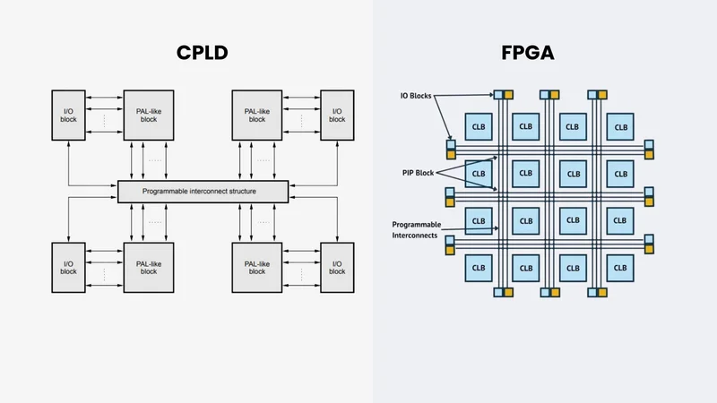
CPLD vs FPGA
Key Takeaways
Fundamental Difference: CPLD uses non-volatile macrocells and a centralized interconnect, while an FPGA uses a distributed array of SRAM-based logic blocks and routing. This leads to instant-on behaviour and deterministic timing for CPLDs but much higher logic capacity and flexibility for FPGAs.
Capacity and Scalability: Modern CPLDs provide up to a few tens of thousands of logic elements (e.g., Lattice MachXO3 with ~9,400 LEs) and are limited by centralized routing, whereas recent FPGAs such as Versal Gen 2 or Agilex 5 contain hundreds of thousands to millions of logic cells with high-speed interfaces.
Configuration and Non-Volatility: CPLDs store their configuration in Flash or EEPROM and retain it when powered down, yielding instant-on operation; FPGAs use SRAM configuration that must be loaded at power-up, though some families integrate on-chip Flash for critical sections.
Timing and Power: CPLDs have consistent propagation delays (~5 ns) and low static power (~50 mW), whereas FPGAs offer higher performance at the cost of higher dynamic power consumption.
Modern Families: The prominent CPLD families include Intel MAX 10, Microchip ATF15xx and Lattice MachXO2/MachXO3/MachXO5; contemporary FPGAs include AMD Versal Gen 2 (with CXL 3.1 and PCIe Gen6 support), Intel Agilex 5 D-Series, and Lattice CrossLink-NX with high memory-to-logic ratios.
Choosing Between Them: Use CPLDs when you need deterministic, low-complexity glue logic, instant-on boot or minimal power. Choose FPGAs when you need large logic capacity, parallel processing, advanced DSP blocks or dynamic reconfiguration capabilities. The decision framework below summarizes typical scenarios.
Introduction
Field-programmable logic devices come in two principal forms, Complex Programmable Logic Devices (CPLDs) and Field-Programmable Gate Arrays (FPGAs). Engineers frequently encounter the CPLD vs FPGA decision when selecting the right hardware for a digital design project. Both device families offer reconfigurable logic, yet they differ significantly in architecture, capacity, power consumption, and cost. Understanding the CPLD vs FPGA distinction is essential for making informed choices that align with performance requirements and budget constraints.
Programmable Logic Devices (PLDs) let designers implement digital circuits without fabricating custom integrated circuits. CPLDs and FPGAs are the principal types of PLDs. The choice between a CPLD vs FPGA often depends on the size of project, timing and configurability requirements. This article presents a comprehensive technical analysis of CPLD vs FPGA, focusing on their architectural distinctions, performance metrics, design flows, and implementation methodologies.
Difference Between a CPLD and an FPGA?
CPLD integrates a modest number of macrocells (clusters of AND-OR logic with flip-flops) connected through a centralized interconnect. The configuration data is stored in non-volatile flash or EEPROM, giving instant-on behaviour. FPGA contains an array of configurable logic blocks built from look-up tables (LUTs) and flip-flops with distributed routing and abundant embedded RAM. FPGAs rely on SRAM configuration that must be loaded at power-up, but they offer far larger logic capacity and flexibility. Because of these fundamental differences, CPLDs excel at deterministic, low-complexity control logic while FPGAs dominate applications requiring large, high-performance digital designs.
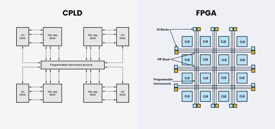
Let’s go through a comparison below:
| Feature | CPLD | FPGA |
| Architecture | Centralized macrocells and programmable interconnect (AND-OR arrays) | Distributed configurable logic blocks (CLBs) with LUTs, flip-flops and rich routing |
| Configuration Memory | Non-volatile (Flash/EEPROM); retains design and powers up instantly | SRAM-based; requires configuration at power-up; some devices include on-chip flash or configuration ROM |
| Logic Capacity | Hundreds to a few tens of thousands of logic elements (e.g., Lattice MachXO3: Up to 9.4k LEs) | Hundreds of thousands to millions of logic cells (AMD Versal Gen 2 and Intel Agilex 5 D-Series exceed 1 M LEs) |
| Timing Predictability | Deterministic propagation delays; suitable for timing-critical control logic | Variable delays; higher clock frequencies and performance but more complex timing closure |
| Power Profile | Low static power (~50 mW) and modest dynamic power | Higher dynamic power due to large routing and logic resources |
| Boot Time | Instant-on; logic is active immediately after power-up | Requires configuration load; boot time can be several seconds |
| Typical Use Cases | Glue logic, system control, interface bridging, industrial controllers, consumer electronics | AI accelerators, signal processing, high-performance computing, networking, aerospace and defence |
| Cost | Lower unit price for small designs | Higher device cost is proportional to capacity, but cost-efficient for complex designs |
What is a CPLD?
Complex Programmable Logic Device (CPLD) is a type of programmable logic that combines multiple Programmable Array Logic (PAL) blocks into a single chip with a centralized interconnect. Each PAL block contains programmable AND and OR planes plus flip-flops, forming macrocells. Because the routing between these macrocells is fixed and deterministic, propagation delays are consistent.
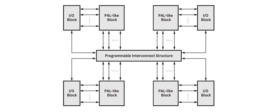
CPLDs typically use flash or EEPROM configuration memory, so they retain their programming even when power is removed. This non-volatile architecture enables instant-on behaviour and makes CPLDs well suited to control and sequencing logic, bootloader enforcement, and low-complexity state machines. [1] However, the centralized routing restricts their scalability and logic capacity to thousands of gates.
Modern CPLD Device Families (2025-2026)
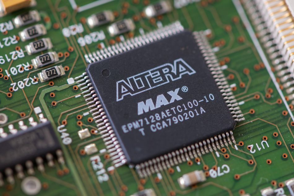
Lattice MachXO3
The Lattice MachXO3 family is commonly used for control PLDs and bridging applications. It provides non-volatile programmable logic with a small footprint and supports densities from 640 to 9,400 LUTs, along with 28 to 384 I/O pins. This makes it suitable for industrial controllers, communication equipment, interface bridging, system monitoring, and low-power glue logic. Lattice also highlights MachXO3 for hardware management and in-system updates through features such as Hitless I/O.
Lattice MachXO5-NX
The Lattice MachXO5-NX family is a newer secure control FPGA family built for higher-density board management and control applications. It extends the traditional CPLD-like role with up to 100K logic density, 7.3 Mb internal memory, 55 Mb user flash memory, PCIe Gen2 support on selected devices, LPDDR4 support, up to 378 programmable I/O pins, and security features such as AES-256 bitstream encryption and authentication. [2] This makes MachXO5-NX useful for secure boot, platform control, data-center hardware management, and root-of-trust applications.
Intel MAX 10
The Intel MAX 10, historically associated with Altera, is best understood as a flash-based FPGA/CPLD hybrid rather than a traditional macrocell CPLD. It integrates configuration flash memory, user flash memory, logic array blocks, ADCs, embedded memory, embedded multipliers, PLLs, and general-purpose I/O. Intel describes MAX 10 devices as instant-on devices suitable for board bring-up, system control, motor control, instrumentation, and mixed-signal embedded applications.
Microchip ATF15xx
The Microchip ATF15xx family represents a more traditional CPLD approach. These devices are flash-based CPLDs designed for low-power, high-performance programmable logic, in-system programming, I/O expansion, bus arbitration, memory interfacing, and legacy PAL/GAL replacement. ATF15xx line includes devices such as the ATF1502AS, which provides 32 macrocells, 32 registers, and 36 I/O pins, making it suitable for simple peripheral control and older digital electronics designs that need long-term support.
Lattice MachXO2
The Lattice MachXO2 family is another crossover programmable logic family often used where engineers previously selected CPLDs. It offers instant-on operation, low standby power, and up to 6,864 LUT4s, making it suitable for board control, bridging, I/O management, and compact embedded systems. Its flash-based architecture and small-package options make it a practical choice for designs that need more flexibility than older CPLDs but less complexity than high-density FPGAs.
What is an FPGA?
Field-Programmable Gate Array (FPGA) is a large array of Configurable Logic Blocks (CLBs) interconnected by a rich, programmable routing network. Each CLB typically contains look-up tables (LUTs) to implement arbitrary logic functions, flip-flops for sequential logic and sometimes dedicated arithmetic blocks. The distributed architecture supports high parallelism and enables designers to build complex digital systems, such as processors, DSP pipelines, and AI accelerators.
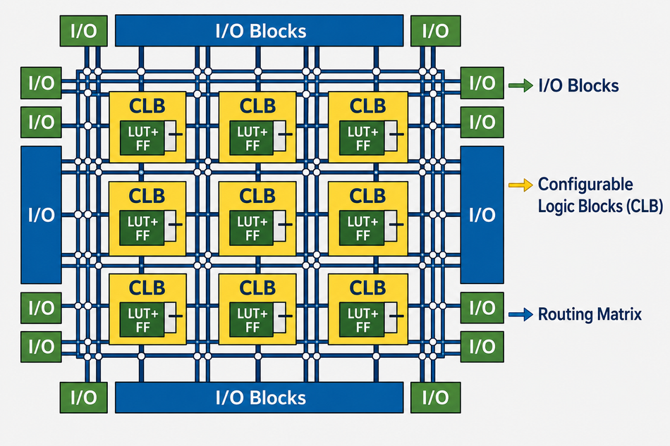
Configuration data is stored in SRAM or on-chip flash; for SRAM-based devices, the bitstream must be loaded from an external memory at power-up, which introduces a short configuration delay but allows dynamic partial reconfiguration.
Modern FPGA Families (2025-2026)
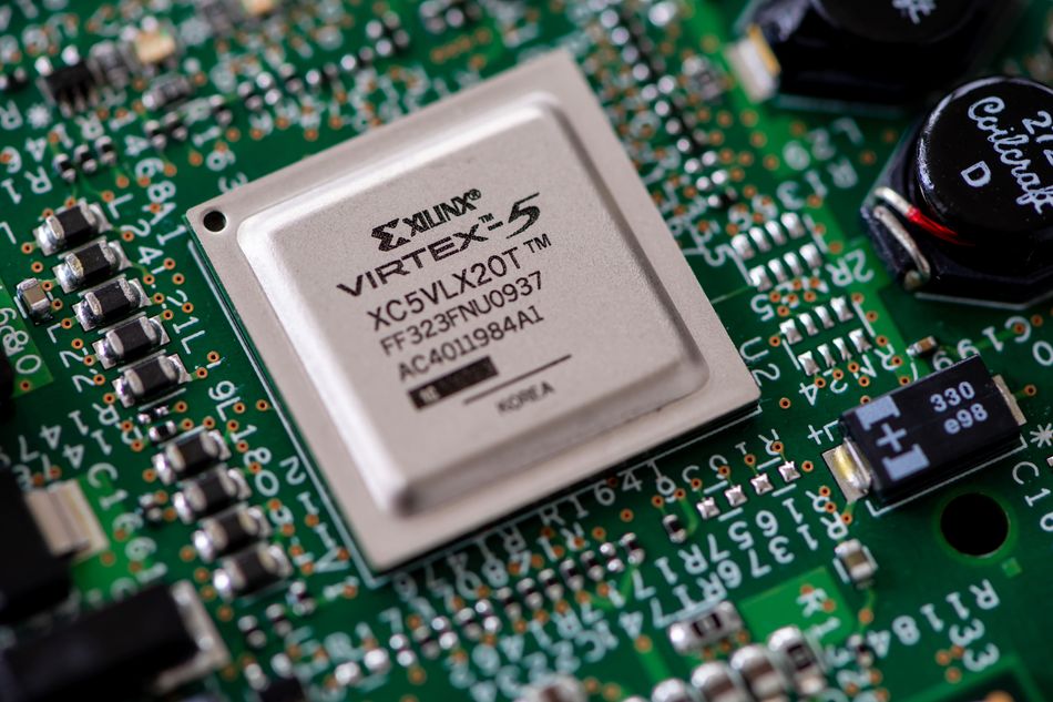
AMD Versal Premium Series Gen 2
The AMD Versal Premium Series Gen 2 targets data-intensive workloads that require high-bandwidth host connectivity and advanced memory support. [3] AMD highlights PCIe Gen6 and CXL 3.1 hard IP, LPDDR5X support up to 8533 Mb/s, DDR5 support up to 6400 Mb/s, and high-speed transceiver capabilities. These devices are aimed at data-center acceleration, storage systems, network infrastructure, test and measurement, and aerospace and defence applications.
AMD Versal Prime Series Gen 2
The AMD Versal Prime Series Gen 2 is designed for embedded systems that need programmable logic combined with strong processing capability. It integrates Arm Cortex-A78AE application processors, Cortex-R52 real-time processors, programmable logic, advanced I/O, hard video encode/decode blocks, and DDR5/LPDDR5X memory controller support. AMD positions this family for video, control, medical imaging, aerospace, defence, software-defined systems, and high-performance embedded computing.
Altera Agilex 5 D-Series
The Altera Agilex 5 D-Series is a mid-range FPGA and SoC FPGA family focused on performance-per-watt, edge AI, video, wireless, and embedded acceleration. Altera states that the expanded Agilex 5 D-Series reaches up to 1.6 million logic elements, supports DDR5 interface speeds up to 5,600 MT/s and LPDDR5 up to 5,500 MT/s, and includes post-quantum cryptography secure boot capability. Altera also introduced Visual Designer Studio in Quartus Prime Software version 25.3 to simplify IP integration and FPGA design entry.
Lattice CrossLink-NX and CrossLinkU-NX
The Lattice CrossLink-NX family is optimized for embedded vision, sensor bridging, and low-power edge applications. Lattice emphasizes small packages, up to 75% lower power versus similar FPGAs, abundant DSP resources, and a high memory-to-logic-cell ratio for AI inferencing. The related CrossLinkU-NX family adds hardened USB support, including USB 2.0 up to 480 Mbps and USB 3.2 up to 5 Gbps, making it useful for camera modules, industrial vision, sensor interfaces, and compact AI-enabled devices.
Lattice CertusPro-NX
The Lattice CertusPro-NX family is a low-power general-purpose FPGA platform built for control, bridging, communications, and edge-processing applications. It offers up to 100K logic cells, 7.3 Mb of embedded memory, 156 18 × 18 multipliers, 299 programmable I/Os, and up to eight SERDES lanes supporting 10.3 Gbps per lane. Lattice also highlights LPDDR4 support, PCIe Gen3, DisplayPort, CoaXPress, AES-256 bitstream encryption, and fast configuration, making CertusPro-NX suitable for machine vision, control-plane bridging, board management, and secure embedded systems.
Recommended Reading: What Is an FPGA? Complete Guide to Field Programmable Gate Arrays for Engineers
Architecture and Key Differences
The core architectural distinction between CPLDs and FPGAs lies in the granularity of logic blocks and the routing fabric:
CPLD Architecture: Macrocells combine programmable AND-OR arrays with flip-flops in a centralized structure. The interconnect is a global bus or crossbar, so delays between any two macrocells are uniform. Because the device uses flash or EEPROM, the configuration is retained when power is removed. However, this centralized routing limits the number of macrocells and reduces flexibility for complex logic. The architecture is well-suited to implementing deterministic glue logic, state machines, and simple combinational circuits.
FPGA Architecture: The distributed grid of Configurable Logic Blocks (CLBs) contains LUTs, flip-flops and often dedicated DSP slices. The routing fabric is segmented and hierarchical, providing numerous paths between blocks but introducing variable delays. FPGAs include multiple types of on-chip memory: distributed RAM within each CLB, Block RAM (BRAM) modules, and, in some cases, UltraRAM or on-chip HBM for high-performance designs. The programmable interconnect, combined with abundant logic and memory resources, enables the implementation of complex pipelines, parallel algorithms and custom processing engines.
Configuration Storage: CPLDs use non-volatile flash/EEPROM, enabling instant-on operation and eliminating the need for external configuration memory. FPGAs typically use SRAM-based configuration, which must be loaded from external flash or configuration ROM at power-up, though some families integrate embedded flash for retaining part of the bitstream. The SRAM approach supports dynamic partial reconfiguration, allowing portions of the design to be updated in the field.
Logic Capacity: The largest CPLDs contain on the order of tens of thousands of equivalent logic gates, whereas modern high-end FPGAs exceed a million logic elements and integrate hardened multi-gigabit transceivers, PCIe controllers and AI engines.
Recommended Reading: What is HBM (High Bandwidth Memory)? Deep Dive into Architecture, Packaging, and Applications
Timing, Power and Performance
Because of their architectural differences, CPLDs and FPGAs exhibit distinct timing and power characteristics:
Propagation Delay and Clock Speed: CPLDs have uniform routing and simplified logic, yielding predictable delays (~5 ns) and clock rates up to 100 MHz. FPGAs, with advanced interconnect and pipelined architectures, achieve faster propagation (~=3 ns) and higher clock frequencies (often 300 MHz or more) but require careful placement and timing analysis.
Power Consumption: Non-volatile CPLDs consume little static power (~=50 mW) and modest dynamic power, making them suitable for battery-powered devices and low-power control logic. SRAM-based FPGAs draw higher static power (~=75 mW) and dynamic power that scales with the number of active logic blocks. Modern FPGAs offer power-saving features such as clock gating, dynamic voltage and frequency scaling (DVFS), and power islands.
Boot Time and Reliability: CPLDs are instant-on and can execute critical boot logic immediately, whereas FPGAs require a configuration sequence that can take from a few milliseconds to several seconds, depending on bitstream size. FPGA designers must consider configuration verification, redundancy and secure boot mechanisms.
Development Tools, HDL Implementation and Debugging
Design flows for CPLDs and FPGAs share similar high-level steps (design entry, synthesis, implementation and verification), but the complexity and tooling differ:
Toolchains (2025-2026)
Lattice Radiant & Diamond: Support MachXO and CrossLink families; Radiant handles Nexus/Avant devices and provides intuitive constraint entry, power analysis and integration with the Propel software for embedded RISC-V processors. Diamond serves legacy MachXO2/MachXO3 devices and provides synthesis and placement for smaller CPLDs.
Intel Quartus Prime v25.3: Supports the Agilex and MAX device families. [4] The 2025 release introduces a Visual Designer Studio, enabling drag-and-drop integration and improved compile times. The design flow includes high-level synthesis (HLS) via OpenCL and oneAPI, as well as support for SystemVerilog and VHDL.
AMD Vivado & Vitis: Vivado targets the Xilinx series (UltraScale+, 7-Series, and Versal) and provides sophisticated floorplanning, timing analysis, and IP integration. The Vitis unified software platform allows the development of heterogeneous applications across CPUs, AI Engines and programmable logic. The upcoming Vitis HLS updates support C++17 and Python-based high-level synthesis.
Microchip Libero SoC: Used for ATF15xx CPLDs and PolarFire FPGAs; integrates constraint management, simulation and open-source synthesis options.
Open-source flows: Tools like Yosys, nextpnr, IceStorm and SymbiFlow provide vendor-neutral synthesis, placement and routing. They support smaller devices such as the Lattice iCE40 and some MachXO families, enabling cost-free experimentation.
Hardware Description Languages
CPLDs: Designs are often described in VHDL or Verilog, focusing on structural and behavioural descriptions of simple state machines and combinatorial logic. Because CPLDs have limited logic capacity and fixed timing, designers minimize logic depth and gate counts.
FPGAs: Support rich HDLs including SystemVerilog, VHDL-2008, Chisel and high-level synthesis languages (C/C++, OpenCL, Python). Designers can instantiate IP cores, use parameterized modules and leverage HLS to accelerate algorithm development.
Configuration Methods
CPLD Configuration: Typically uses JTAG in-system programming (ISP). The bitstream is stored in on-chip flash or EEPROM, so configuration is fast (sub-second) and persistent. Security features include fuse bits and simple encryption.
FPGA Configuration: Supports multiple interfaces, JTAG, SPI, PCIe and parallel flash. Large FPGAs can take several seconds to configure. They often support partial reconfiguration, where specific regions of the logic fabric can be updated without stopping the entire device. Advanced devices offer bitstream encryption, authentication and tamper detection.
Debugging Features
Both CPLDs and FPGAs integrate debugging primitives:
Integrated Logic Analyzers (ILA): Provide real-time signal capture and viewing within the device fabric.
Boundary-scan (JTAG) Test: Allows probing of I/O and internal nodes without physical access.
Hardware Breakpoints and Triggers: Useful for capturing specific sequences during operation.
Power and Performance Monitors: Available in higher-end FPGAs, they help optimize power budgets and analyze dynamic behaviour.
Recommended Reading: FPGA Development: Architecture, Tools, and Design Flow
Use Cases and Applications
CPLD Applications
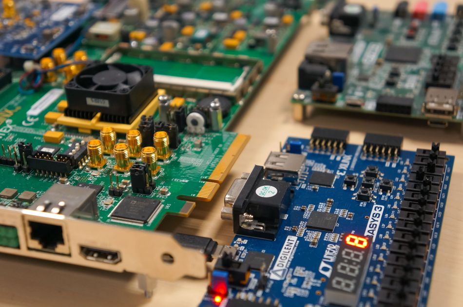
CPLDs continue to serve niche roles where deterministic timing, instant-on control and small logic capacity are critical. Flash-based CPLDs remain important for logic consolidation, system monitoring and safety interlock logic, especially when devices must be active immediately at power-up. Typical applications include:
Industrial Controllers: Manage state machines and timing for factory automation and robotics. The non-volatile memory of CPLD ensures reliable operation during power outages.
Glue Logic and Protocol Bridging: Convert between incompatible bus standards (e.g., SPI-to-GPIO, address decoding, chip-select generation). The simple architecture allows quick integration into board designs.
Consumer Electronics: Implement low-power control in appliances, digital displays and I/O controllers where cost and fast start-up matter.
Secure Boot and System Management: Provide small, tamper-resistant control logic for larger FPGA or microprocessor systems; for example, enforcing boot loader access and watchdog timers in networking equipment.
FPGA Applications
FPGAs excel at high-performance and parallel workloads. Modern applications include:
High-Performance Computing and AI Acceleration: FPGAs implement deep-learning inference engines, digital signal processing chains and custom tensor accelerators. Cloud platforms (AWS, Azure) offer FPGA instances for data-center acceleration. AMD's Versal Premium Gen 2 supports CXL 3.1 and PCIe Gen6 to deliver high-bandwidth host connectivity and memory pooling.
Telecommunications: FPGAs perform baseband processing for 5G/6G radios, modulation/demodulation, error correction and protocol translation. [5] Their reconfigurability allows upgrades to new standards without hardware replacement.
Aerospace and Defence: Provide deterministic, high-throughput processing for radar, sonar and mission-critical systems. The partial reconfiguration of FPGA enables adaptive algorithms and dynamic redundancy.
Embedded Vision and Edge AI: CrossLink-NX bridges image sensors to processors and includes dedicated multipliers for inference acceleration; devices offer integrated USB 3.2 and PCIe Gen2 IP.
Recommended Reading: What are FPGAs used for? A Deep Dive Into Architecture, Advantages, and Modern Applications
Decision Framework: When to Use a CPLD vs an FPGA?
Choosing between a CPLD and an FPGA depends on system requirements.
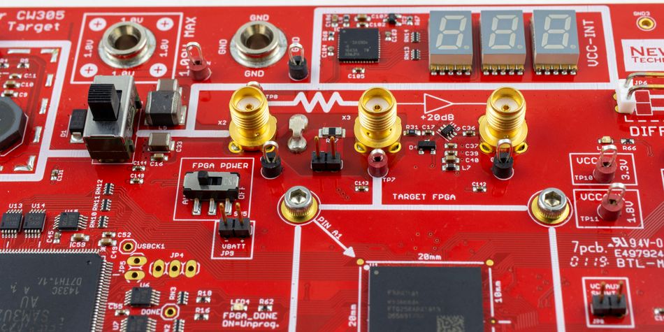
The following scenarios outline typical considerations:
Use a CPLD for Simple Glue Logic and State Machines
CPLD is a strong choice for glue logic, address decoding, reset control, watchdog circuits, and small sequential logic designs. Its macrocells, flip-flops, centralized interconnect, and predictable routing make timing easier to control. For designs that need only a few thousand logic gates, a CPLD usually offers lower power consumption, lower cost, and faster startup than an FPGA.
Use a CPLD for Instant-On Safety and System Management
If the system must become active immediately after power-up, a CPLD is often the safer option. Most CPLDs use non-volatile memory, such as Flash or EEPROM, so the configuration remains stored even when power is removed. This makes CPLDs suitable for power sequencing, secure boot enforcement, board management, I/O supervision, and safety-related control logic. Older PLDs, including PAL, PLA, and SPLD devices, served similar roles, but modern CPLDs provide higher integration and better flexibility.
Use an FPGA for DSP, AI, and High-Performance Processing
FPGA should be selected when the design requires high logic capacity, parallel processing, embedded memory, multipliers, PLLs, and high-speed datapaths. FPGAs use configurable logic blocks (CLBs) built around lookup tables (LUTs), flip-flops, and programmable routing. This architecture makes them suitable for digital signal processing, video processing, machine learning, artificial intelligence, networking, and complex embedded systems.
Use an FPGA for High-Bandwidth Interfaces
High-speed interfaces such as PCIe, Ethernet, CXL, JESD204, and advanced memory controllers generally require an FPGA. Vendors such as AMD and Altera provide FPGA families with hardened transceivers, high-speed I/O, SRAM-based configuration, and advanced toolchains. Although SRAM-based FPGAs require configuration at startup, they offer far greater flexibility and performance than CPLDs.
Use an FPGA for ASIC Prototyping
For ASIC or application specific integrated circuits development, an FPGA is usually the preferred prototyping platform. Engineers can describe the design using hardware description languages (HDLs) such as VHDL and Verilog, then use synthesis, place and route, and timing analysis to validate the architecture before silicon fabrication. This makes FPGAs essential for complex digital electronics verification.
Use a CPLD-FPGA Hybrid for Mid-Range Designs
Some devices sit between traditional CPLDs and FPGAs. Families such as Intel MAX 10, Lattice MachXO, and older CoolRunner devices combine instant-on behaviour, programmable I/O pins, embedded memory, and moderate logic resources. These hybrid devices are useful when a design needs more flexibility than a simple programmable logic device, but less complexity than a high-end FPGA.
Recommended Reading: Verilog vs VHDL: A Comprehensive Comparison
Conclusion
The CPLD vs FPGA choice depends on logic capacity, timing predictability, power consumption, startup behavior, and cost. CPLDs remain ideal for glue logic, deterministic control, power sequencing, and instant-on boot because their non-volatile macrocell architecture keeps configuration available at power-up. FPGAs are better for complex digital systems that require LUT-based logic, parallel processing, embedded memory, DSP blocks, high-speed interfaces, and AI acceleration. By understanding the difference between non-volatile CPLD macrocells and SRAM-based FPGA fabrics, engineers can match each device to the right application, reduce design risk, and build more efficient, scalable, and reliable hardware. This practical framework also supports long-term maintainability across evolving embedded platforms.
Frequently Asked Questions
Q. Are CPLDs still used today?
A. Yes. CPLDs are still used for glue logic, system monitoring, safety interlocks, power sequencing, and board management. Their instant-on operation, low power consumption, compact packages, and non-volatile memory make them useful in many modern embedded systems.
Q. Is FPGA technology outdated?
A. No. FPGA technology is still highly relevant in digital electronics, AI acceleration, networking, automotive systems, aerospace, industrial automation, and video processing. Modern FPGAs offer high-speed interfaces, embedded memory, DSP blocks, security features, and strong parallel processing capability.
Q. What are the disadvantages of using a CPLD?
A. CPLD has lower logic capacity than an FPGA and fewer embedded resources such as memory, multipliers, PLLs, and advanced routing. It is not suitable for large digital signal processing, machine learning, or data-intensive hardware designs.
Q. What is the difference between PLA, PAL, CPLD and FPGA?
A. PLA and PAL devices are early programmable logic devices for small logic functions. A CPLD combines multiple PAL-like blocks with programmable interconnect. FPGA uses LUT-based configurable logic blocks, distributed routing, and higher capacity for complex digital systems.
Q. Do CPLDs require external configuration memory?
A. Usually, no. Most CPLDs store their configuration in on-chip non-volatile memory, such as Flash or EEPROM. This allows instant-on operation after power-up, unlike many SRAM-based FPGAs that require an external configuration memory or boot source.
Q. What happens to CPLD users now that AMD discontinued CoolRunner II?
A. Designers using AMD CoolRunner II should plan migration carefully. Common alternatives include Lattice MachXO2, MachXO3, and Microchip ATF15xx CPLDs. Pin compatibility, timing behavior, voltage levels, package availability, and toolchain support should be checked before replacement.
Q. Is there a middle ground between CPLDs and FPGAs?
A. Yes. Devices such as Intel MAX 10 and Lattice MachXO families combine CPLD-like instant-on behavior with FPGA-style LUTs, embedded memory, I/O flexibility, and higher logic capacity, making them useful for bridging, control, and moderate embedded processing.
References
[1] Promwad. CPLD Trends: Analysis of Developments and the Impact of Discontinued AMD FPGA and CPLD Lines [Cited 2026 July 05]; Available at: Link
[2] Lattice Semiconductor. MachXO5-NX: Advanced Secure Control FPGA Documentation [Cited 2026 July 05]; Available at: Link
[3] HPCwire. AMD Enhances Data Center and Edge Performance with Versal Premium Series Gen 2 SoCs [Cited 2026 July 05]; Available at: Link
[4] Embedded Computing Design. Altera - Agilex FPGA Portfolio Now in Full Production with Major Performance Upgrades [Cited 2026 July 05]; Available at: Link
[5] Logic Fruit Technologies. Future of FPGAs - Industry Trends & Market Growth (2026) [Cited 2026 July 05]; Available at: Link
in this article
1. Key Takeaways2. Introduction3. Difference Between a CPLD and an FPGA?4. What is a CPLD?5. What is an FPGA?6. Architecture and Key Differences7. Timing, Power and Performance8. Development Tools, HDL Implementation and Debugging9. Use Cases and Applications10. Decision Framework: When to Use a CPLD vs an FPGA?11. Conclusion12. Frequently Asked Questions13. References