IGBT: Insulated Gate Bipolar Transistor Guide
Engineering reference for high voltage, high-current power conversion.

27 Jun, 2026. 12 minutes read
Key Takeaways
An IGBT, or insulated gate bipolar transistor, combines a MOSFET-like insulated gate with a conductivity-modulated bipolar output path, making it valuable for high-voltage, high-current switching.
IGBTs are strongest in medium-switching-frequency power electronics, especially motor drives, solar inverters, UPS systems, induction heating, and industrial power conversion.
The core trade-off is a lower on-state saturation voltage versus higher switching losses than MOSFETs, mainly because minority carriers create tail current during turn-off.
Gate drive design is critical. Typical high-power IGBT gate drives use about +15 V turn-on and 0 V, -5 V, or -15 V turn-off, with Miller control, desaturation protection, and careful layout.
The antiparallel freewheeling diode is not optional in inductive converter legs. It defines current continuity, diode recovery loss, EMI behavior, and safe half-bridge commutation.
SiC MOSFETs are increasingly preferred where high switching speed, high switching frequency, and compact magnetics justify cost, while IGBTs remain cost-effective in many high-power inverters.
Introduction
The IGBT is one of the central switching devices in modern power electronics. The full name, insulated gate bipolar transistor, describes its hybrid character: it is driven through an insulated MOS gate like a power MOSFET, but its main collector-emitter current path behaves more like a bipolar device when it is on. That combination gives the IGBT high input impedance, relatively simple voltage-mode drive, and strong high-voltage, high-current capability.
Engineers usually select IGBTs when silicon MOSFETs become inefficient at high blocking voltages and when a BJT would require excessive base drive. The device is common in variable-frequency drives, servo drives, traction inverters, electric-vehicle power stages, electric cars, rectifier-linked inverter systems, solar inverters, induction heating, uninterruptible power supply equipment, air conditioners, microwave ovens, and other home appliances. Toshiba describes IGBTs as voltage-controlled devices that switch power between collector and emitter, and its product material lists home appliances through infrastructure equipment as application areas.
This article focuses on what an IGBT is, how it works, how it differs from MOSFETs and BJTs, and how to implement it in real power conversion hardware.
What Is an IGBT?
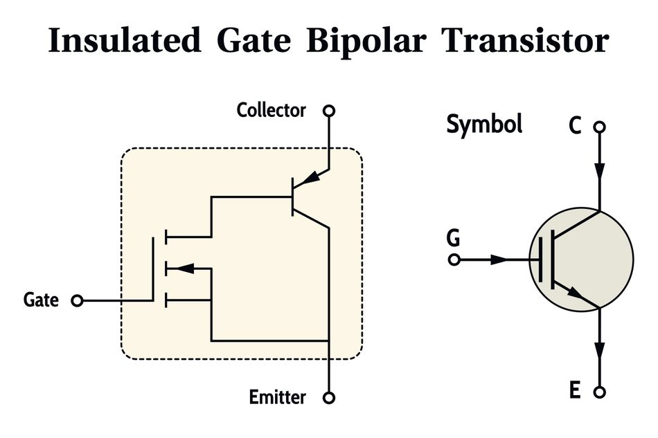
An IGBT is a three-terminal power semiconductor with a gate, collector, and emitter. In most power conversion applications, the device is an N-channel IGBT used as a controlled switch. A positive gate-emitter voltage forms an MOS channel that enables carrier injection into the drift region. The collector-emitter path then conducts via conductivity modulation, reducing the effective drift-region resistance compared with that of a high-voltage silicon MOSFET.
The simplest mental model is: MOSFET input, bipolar output. The gate is insulated by oxide, so the steady-state input current is very small, apart from leakage. The gate driver must still source and sink significant transient current because the gate-emitter and Miller capacitances must be charged and discharged quickly.
The collector and emitter are not interchangeable, unlike the somewhat more symmetric source-drain conduction behavior designers may use in low-voltage MOSFET circuits.
In standards and datasheets, IGBT ratings and measurements are treated with the same rigor as those for other power semiconductor devices. IEC 60747-9:2019 specifies terminology, letter symbols, essential ratings, characteristics, rating verification, and measurement methods for insulated gate bipolar transistors.
Suggested Reading: SiC MOSFET: Wide-bandgap Power Devices for High-Efficiency Converters
Internal Structure, Thyristor Structure, and Latch-Up
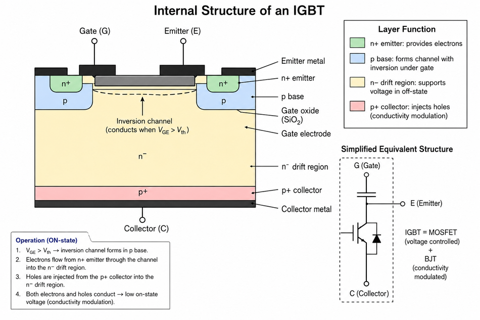
A conventional IGBT has a layered semiconductor stack that includes a p+ collector, an n-drift region, a p-base, and an n+ emitter. It’s similar to a MOSFET, with an additional p+ drain-side region that creates four alternating p-n-p-n layers. Current flows through an internal PNP transistor when the MOS channel is turned on and a collector-emitter voltage is applied.
When the gate-emitter voltage exceeds the threshold, an inversion channel forms in the p-base region. Electrons are injected from the emitter side, while holes are injected from the p+ collector into the n- drift region.
This stored charge creates conductivity modulation, which lowers the on-state voltage. That is why an IGBT can be attractive at high voltage and high current, where the drift-region resistance of a silicon MOSFET becomes large.
The same minority-carrier physics creates the turn-off limitation. When the channel turns off, carriers stored in the drift region must recombine or be removed. This produces tail current, which extends turn-off energy and reduces switching speed compared with MOSFETs.
The p-n-p-n structure also implies an internal thyristor structure. A parasitic thyristor exists because the internal PNP and NPN transistor paths can create regenerative feedback. If this parasitic thyristor turns on, the gate loses control, and the device enters latch-up.
Modern IGBT cell design, emitter shorts, optimized p-base resistance, and safe operating area limits make latch-up uncommon in properly designed systems, but latch-up is still a failure mode engineers must respect.
For implementation, do not treat latch-up as a theoretical curiosity. Use a gate driver with desaturation protection, enforce current limits in firmware and hardware, keep stray inductance low, and stay within the datasheet safe operating area.
Operating Regions, Conduction Loss, and Switching Losses
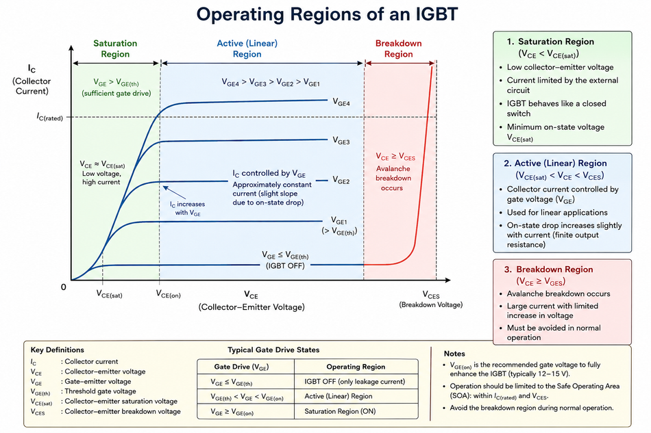
In power electronics, the IGBT is typically used as a switch rather than as a linear amplifier. Its practical operating states are off-state blocking, turn-on transition, on-state conduction, turn-off transition, and diode conduction during reverse or freewheel current. The intended operating region is either fully off or fully enhanced, with minimum time spent in the high-voltage, high-current overlap region.
The on-state voltage is specified as the collector-emitter saturation voltage, written VCE(sat). This saturation-voltage characteristic is not purely resistive, unlike MOSFET RDS(on). It has a diode-like offset plus slope resistance, and it varies with collector current, gate voltage, and junction temperature. A quick conduction estimate is:
Pcond ≈ VCE(sat) × Iavg during conduction
For sinusoidal motor control, space-vector PWM, or discontinuous current modes, engineers should integrate the instantaneous voltage and current over the switching period rather than relying on a single average value.
Switching losses are usually handled with datasheet energy parameters: Eon, Eoff, and sometimes Erec for the freewheeling diode. Infineon's IGBT characteristics note explains that switching energy is characterized in datasheets by temperature, collector current, and gate resistance, and that double-pulse testing is commonly used to measure clamped inductive load.
A common first-order estimate is:
Psw ≈ fsw × (Eon + Eoff + Erec)
This equation is only a starting point. In real hardware, switching losses depend on DC-link voltage, collector current, junction temperature, gate resistance, stray inductance, diode recovery, snubbers, and switching frequency.
A real module illustrates the scale. The Infineon FF600R12ME4 EconoDUAL 3 module is a 1200 V, 600 A IGBT module using Trench/Fieldstop IGBT4 technology with an emitter-controlled diode and NTC.
Its datasheet lists typical VCE(sat) of 1.75 V at 600 A, VGE = 15 V, and Tvj = 25 °C, rising to about 2.05 V at Tvj = 150 °C. At 600 A, VCC = 600 V, VGE = ±15 V, RG = 1.5 ohm, and Tvj = 150 °C, the datasheet lists Eon = 90 mJ, Eoff = 79.5 mJ, and the reverse-recovery energy Erec = 51 mJ.
That example shows why thermal design dominates high-power inverter engineering. If those exact switching energies were repeated at 5 kHz in a single switch position, the switching-energy term alone would be about 1.1 kW before accounting for conduction loss, gate-driver loss, diode conduction, and thermal spreading. In an actual inverter, current waveform, modulation index, phase angle, dead time, and device sharing determine the real per-device loss.
Recommended Reading: How Do MOSFETs Work: Comprehensive Technical Guide for Engineers (2025)
Gate Drive, Half-Bridge Control, and Protection
The IGBT gate is voltage-controlled but not a logic input. Gate-drive design sets switching speed, switching losses, EMI, short-circuit behavior, and false-turn-on margin. High-power IGBT gate drives often use +15 V turn-on and negative turn-off voltage, such as -5 V or -15 V. Infineon's characterization note states that high-power gate drive circuits may swing from +15 V to -5 V or -15 V to improve noise immunity and switching performance.
Gate-emitter absolute maximum voltage is commonly ±20 V, but designers must verify the selected device. The FF600R12ME4 datasheet, for example, lists VGES = ±20 V, gate charge of 4.4 microcoulombs at VGE = ±15 V and VCC = 600 V, and input capacitance of 37 nF under its stated test conditions.
A practical IGBT gate-drive stage normally includes:
A dedicated isolated gate driver for each high-side and low-side device in a half-bridge.
Separate turn-on and turn-off resistors when independent control of di/dt and dv/dt is needed.
A low-inductance gate-emitter loop, often with Kelvin emitter sensing in power modules.
Active Miller clamp or negative gate bias to prevent dv/dt-induced turn-on.
Desaturation detection and soft shutdown for short-circuit faults.
Undervoltage lockout prevents the IGBT from operating with insufficient gate voltage.
Carefully controlled dead time between complementary devices in a half-bridge.
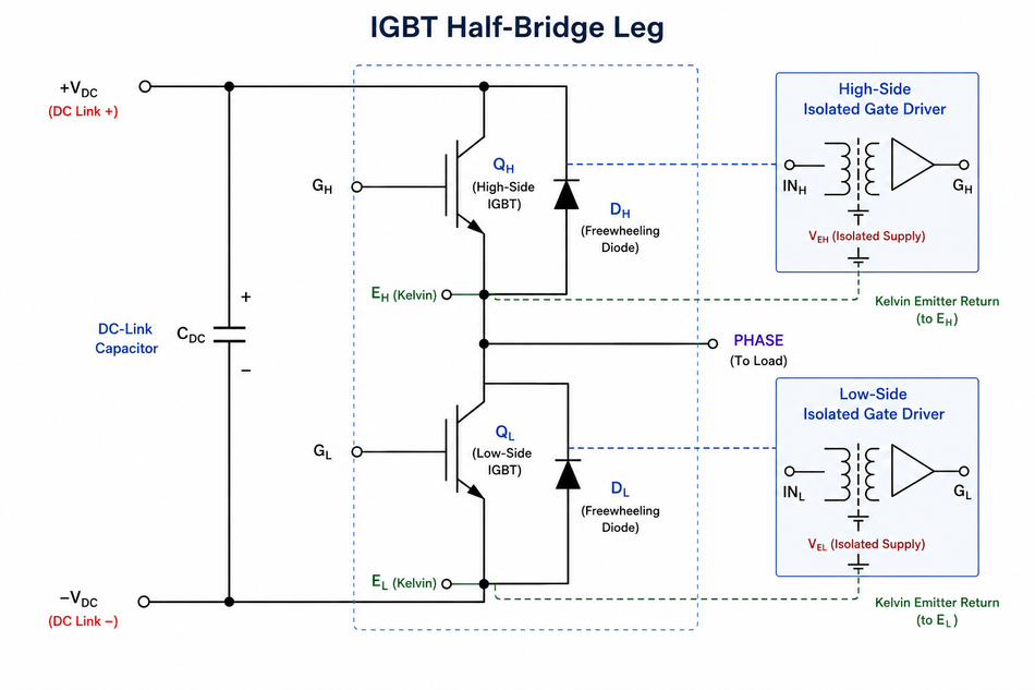
The half-bridge is the fundamental building block for motor drives, inverters, UPS stages, and many DC-link power conversion systems. A three-phase inverter uses three half-bridge legs. Each leg connects the motor phase to either the positive or negative direct-current bus via a controlled IGBT. During dead time or inductive current reversal, current commutates through the antiparallel freewheeling diode or a reverse-conducting device structure.
Freewheeling Diode, Rectifier Stages, and Power Modules
An IGBT does not conduct reverse current like a MOSFET body diode. In inverter legs that drive inductive loads, an antiparallel freewheeling diode is used to provide a current path when the IGBT turns off or when the phase current reverses. In many IGBT modules, the diode is co-packaged and matched to the transistor. Its forward voltage, reverse-recovery charge, softness, and thermal resistance are part of the converter's loss budget.
The freewheeling diode is especially important in motor control. A motor winding current cannot change instantaneously, so the diode supports current continuity during PWM transitions. Poor diode recovery increases switching losses, voltage overshoot, EMI, and stress on the opposite IGBT during turn-on.
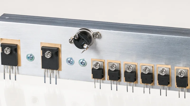
IGBT modules package one or more switches, diodes, isolation substrates, terminals, and often an NTC thermistor into a mechanically robust power module. Infineon describes IGBT modules as available in configurations such as chopper, dual, PIM, four-pack, six-pack, twelve-pack, 3-level, booster, and single-switch modules.
Recommended Reading: Motor Controller: Types, Design Considerations, Control Strategies, and Selection for Engineers
Common module formats include:
Module format | Typical use | Engineering note |
Single switch | Chopper, braking switch, boost switch | Simplest thermal and layout partitioning |
Dual half-bridge | Phase leg, DC/DC bridge, inverter leg | Common in high-power modular inverter design |
Six-pack | Three-phase motor drives and motor control | Compact, but thermal coupling must be modeled |
PIM or CIB | Rectifier, inverter, and brake in one package | Useful for VFD and appliance inverter platforms |
3-level module | NPC, T-type, solar inverters, UPS | Lower device voltage stress and lower output ripple |
Power module with NTC | Industrial drives and converters | Allows local temperature estimation but not direct junction measurement |
A rectifier often creates the DC link from AC mains, after which IGBTs synthesize a controlled AC waveform for motors, transformers, or grid-tied power conversion. In higher-performance systems, the front-end rectifier may itself become an active IGBT or SiC power stage to control power factor and regenerative energy flow.
IGBT vs MOSFETs vs BJT vs SiC MOSFETs
The IGBT competes with silicon MOSFETs, BJTs, thyristors, and SiC MOSFETs. The right device depends on blocking voltage, RMS current, switching frequency, thermal limits, short-circuit requirements, cost, and the control strategy.
Device | Input drive | Conduction behavior | Switching speed | Best fit | Main limitation |
IGBT | Voltage-driven insulated gate, high input impedance | VCE(sat) with conductivity modulation | Medium, limited by tail current | High voltage, high-current inverters, motor drives, UPS, solar inverters | Higher turn-off switching losses than MOSFETs |
Silicon MOSFETs | Voltage-driven insulated gate | Resistive RDS(on), no minority-carrier storage | Fast | Low to medium voltage, high switching frequency, DC/DC converters | RDS(on) rises strongly as voltage rating increases |
BJT | Current-driven base-emitter junction | Saturation voltage, minority-carrier storage | Slower than modern MOSFETs and many IGBTs | Legacy high-current circuits, niche linear or switching designs | Requires continuous base drive and has harder paralleling |
SiC MOSFETs | Voltage-driven gate, wider-bandgap device | Majority-carrier, low high-voltage resistance | Fast | High efficiency, high voltage, high switching frequency, compact magnetics | Higher cost, stricter gate and layout requirements |
The practical selection rule is straightforward. Choose silicon MOSFETs when the voltage is low enough that RDS(on) is acceptable and the switching frequency is high. Choose an IGBT when voltage and current are high, switching frequency is moderate, and cost per kilowatt matters.
Choose SiC MOSFETs when higher switching frequency, higher temperature operation, lower switching losses, or smaller magnetics justify the cost and layout complexity.
Device Selection by Application
Application | Common power stage | Typical device direction | Why an IGBT may fit |
Industrial VFD and motor drives | Three-phase inverter from a rectified DC link | 650 V, 1200 V, or 1700 V IGBT modules | Robust motor control, mature gate drivers, strong overload capability |
Servo drives and robotics | Three-phase inverter, often compact | Discrete IGBTs or six-pack power modules | Good efficiency at moderate switching frequency |
Electric vehicle traction inverter | Three-phase inverter | IGBT modules or SiC MOSFET modules | IGBTs remain viable in cost-sensitive electric vehicle platforms, while SiC improves efficiency and power density |
Solar inverters | Boost, inverter, or 3-level topology | IGBTs, SiC MOSFETs, or hybrid modules | Good for high voltage DC links and grid-frequency power conversion |
UPS | Rectifier, DC/DC, inverter | 650 V to 1200 V IGBTs or modules | Mature short-circuit protection and high surge capability |
Induction heating | Resonant or quasi-resonant inverter | Soft-switching IGBT or RC-IGBT | Handles high resonant voltage and cost-sensitive appliance power |
Air conditioners | PFC plus compressor inverter | Discrete IGBTs, IPMs, or power modules | Efficient motor control and compact power stage |
Microwave ovens and home appliances | Resonant inverter or motor drive | Discrete IGBT or RC-IGBT | Good fit for high voltage resonant switching and cost control |
For induction heating appliances, Toshiba notes that IGBT switches are common in rice cookers, cooking hobs, milk frothers, and hot plates. It also gives a useful design warning: in single-ended parallel resonant converters, the peak IGBT voltage may be 900 V to 1200 V from a 100 VAC supply and 1350 V to 1800 V from a 220 VAC supply, before accounting for additional transient margin.
For high-power industrial modules, the Infineon FF600R12ME4 example shows how datasheet information should be read as a complete system: VCES, DC collector current, VCE(sat), switching energy, diode recovery energy, gate charge, thermal resistance, stray inductance, isolation, and application notes all matter. A power module is not selected only by voltage and current.
Practical Implementation Checklist
Start with voltage margin. A 400 VAC industrial rectifier creates a DC link near 565 V before line tolerance and regeneration. A 690 VAC system produces a much higher DC link voltage. In practice, this is why 1200 V and 1700 V IGBT modules are common in industrial motor drives. For electric cars and high-voltage batteries, select the device class after accounting for the maximum battery voltage, load-dump behavior, DC-link overshoot, insulation coordination, and fault conditions.
Next, model both conduction loss and switching losses. Use datasheet Eon, Eoff, and Erec values corrected for current, voltage, temperature, and gate resistance. For motor control, evaluate losses over torque, speed, modulation index, and cooling conditions. Thermal impedance curves are more useful than steady-state thermal resistance when overloads or pulsed currents are expected.
The layout is part of the power device. Keep the commutation loop short, use laminated busbars or tightly coupled planes where possible, and separate the power emitter from the Kelvin emitter in the gate loop. High di/dt in a half-bridge can create a voltage across the stray inductance that either slows switching or unintentionally drives the gate.
Finally, validate the converter with a double-pulse test before assuming it is production-ready. Measure voltage overshoot, current fall and rise, diode recovery, gate-emitter ringing, collector-emitter dv/dt, desaturation trip time, and case temperature.
Conclusion
The IGBT remains a foundational power semiconductor because it solves a practical engineering problem: efficient high-voltage, high-current switching with a gate interface that is easier than that of a BJT and often more economical than SiC MOSFETs. Its insulated gate provides high input impedance, while its bipolar conduction path lowers the saturation voltage in applications where silicon MOSFETs would suffer excessive drift.
The main design tradeoff is switching speed. The tail current increases switching losses and limits switching frequency, so IGBT power conversion is usually optimized around moderate-frequency PWM, careful gate drive, and robust thermal design. The freewheeling diode, half-bridge layout, desaturation protection, and power module package are as important as the silicon die.
FAQ
1. What is an IGBT in simple engineering terms?
An IGBT is a power switch with a MOSFET-like insulated gate and a bipolar collector-emitter conduction path. The gate controls whether current can flow from the collector to the emitter. Because the gate is insulated, the driver primarily charges and discharges the capacitance rather than supplying a continuous base current, as in a BJT. The device is widely used when high voltage and high current must be switched efficiently at a moderate switching frequency.
2. Why use an IGBT instead of MOSFETs?
Use an IGBT when the bus voltage and current are high enough that a silicon MOSFET's RDS(on) becomes inefficient or expensive. The IGBT uses conductivity modulation to reduce the on-state voltage in high-voltage devices. MOSFETs still win at low voltage and high switching frequency because they are majority-carrier devices with faster switching and no tail current. SiC MOSFETs change the boundary, but cost and design complexity still matter.
What causes IGBT switching losses?
IGBT switching losses occur because voltage and current overlap during turn-on and turn-off. Turn-off is especially important because minority carriers stored in the drift region create tail current after the MOS channel turns off. Datasheets usually provide Eon and Eoff under specified current, voltage, gate resistance, and temperature. In a half-bridge, diode reverse recovery energy can also be a major part of total switching loss.
3. Does every IGBT need a freewheeling diode?
In most inductive switching applications, yes. Motor drives, solenoid drivers, inverters, UPS stages, and induction heating circuits need a current path when the IGBT turns off. That path is usually an antiparallel freewheeling diode, either discrete or co-packaged in an IGBT module. Some reverse-conducting IGBTs incorporate reverse-conduction capability, but the designer must still analyze reverse recovery, current rating, and thermal stress.
4. What gate voltage should an IGBT use?
Many high-power IGBTs are driven at about +15 V for turn-on. Turn-off may use 0 V in simpler systems or a negative voltage such as -5 V or -15 V where dv/dt immunity is important. The exact values must come from the datasheet and gate driver design. Engineers must also respect the gate-emitter maximum rating, commonly ±20 V, and control gate ringing so transients do not exceed limits.
5. What is IGBT latch-up?
Latch-up is a loss of gate control caused by the internal parasitic thyristor turning on. The IGBT contains p-n-p-n layers that can behave like a thyristor structure if internal regenerative feedback becomes strong enough. Modern devices are designed to suppress latch-up, but unsafe current, temperature, dv/dt, or operation outside the safe operating area can still create risk. Proper gate drive, fast overcurrent protection, and layout are the mitigation tools.
References
IEC, IEC 60747-9:2019, Semiconductor Devices, Part 9: Insulated-Gate Bipolar Transistors (IGBTs).
Toshiba Electronic Devices & Storage, IGBTs (Insulated Gate Bipolar Transistor) Application Note.
Infineon Technologies, AN-983: IGBT Characteristics.
Infineon Technologies, AN-990: Characterization of IGBTs.
Infineon Technologies, IGBT Modules Portfolio and FF600R12ME4 Datasheet.
ROHM Semiconductor, SiC Power Devices Application Note
in this article
1. Introduction2. What Is an IGBT?3. Internal Structure, Thyristor Structure, and Latch-Up4. Operating Regions, Conduction Loss, and Switching Losses5. Gate Drive, Half-Bridge Control, and Protection6. Freewheeling Diode, Rectifier Stages, and Power Modules7. IGBT vs MOSFETs vs BJT vs SiC MOSFETs8. Device Selection by Application9. Practical Implementation Checklist10. Conclusion11. FAQ12. References