DC to AC Inverter Circuits – Theory, Design and Practical Implementation
Modern electronics and renewable energy systems depend on DC to AC inverters that convert a DC source into a clean sinusoidal AC output. This technical article explains the theory behind inverter circuits, their types, architectures, and practical design tips.

06 Oct, 2025. 13 minutes read

Key takeaways
A DC-to-AC inverter converts DC input into an AC output and is classified as voltage-source or current-source by input impedance.
Single-phase inverters use two switches with a split DC source (half-bridge) or four switches in an H-bridge (full-bridge); full-bridge outputs double the RMS voltage of half-bridge.
Sinusoidal PWM generates gating signals by comparing a sinusoidal reference to a high-frequency triangular carrier, allowing precise output voltage control and lower harmonics.
Three-phase inverters use six switches to create three sinusoidal outputs 120° apart; conduction mode (180° or 120°) affects switch conduction, voltage use, and harmonics.
Pure sine-wave inverters reach 90–95% efficiency, modified sine-wave units have 75–85%, and multi-level inverters enhance harmonic quality and efficiency.
Introduction
Inverters are the heart of modern power electronics. Whether powering an uninterruptible power supply (UPS), driving a motor or interfacing renewable‑energy sources to the grid, the inverter converts a direct current (DC) source into a controlled alternating current (AC) output. Digital design engineers, hardware engineers and electronics students need a deep understanding of inverter circuits to design efficient and reliable systems.
This article provides an in‑depth exploration of DC–to–AC inverters, from fundamental theory to practical implementation. It explains how various topologies synthesize AC waveforms, the role of control strategies like pulse‑width modulation, and how component choices influence efficiency and harmonic performance. The discussion extends to multi‑phase and multi‑level inverters that enable high‑power applications and grid‑connected renewable energy systems. By the end, you will be equipped with both theoretical insight and practical guidance to design your own inverter circuits.
Suggested Reading: Power Management for Tomorrows Innovations
Fundamentals of DC–to–AC conversion
How Inverters Work
An inverter converts DC power into AC power by rapidly switching semiconductor devices to produce an alternating voltage across the output terminals. The switching network periodically reverses the polarity of the DC supply or modulates the duty cycle so that the time‑average output voltage varies sinusoidally.
For power engineers, a fundamental distinction is between voltage‑source inverters (VSI) and current‑source inverters (CSI):
Voltage‑source inverter (VSI): The DC input has low impedance. The inverter synthesizes a desired AC output voltage waveform. Modern VSIs use MOSFETs or insulated‑gate bipolar transistors (IGBTs) and do not require commutation circuits because these devices are self‑commutating.
Current‑source inverter (CSI): The DC source has high impedance and the inverter delivers a controlled AC. Thyristor‑based CSIs require forced commutation circuits to turn off the thyristors. CSIs are common in high‑power industrial drives.
This article will focus on VSIs because they dominate contemporary designs.
Ideal Square‑wave Conversion
The simplest inverter produces a square‑wave output by alternately connecting the load to the positive and negative terminals of the DC source. Square‑wave inverters are easy to implement, but they have significant harmonic distortion—about 48 % total harmonic distortion (THD)—and are unsuitable for sensitive loads without additional filtering.
Consequently, square‑wave topologies are mainly used in low‑cost applications or in motor drives where the load’s inductance filters the harmonics.
Single‑phase inverter topologies
Single‑phase inverter circuits form the basis for more complex three‑phase and multi‑level architectures. They can be realized in two fundamental topologies:
Half‑bridge
Full‑bridge.
Half‑bridge inverter
A single‑phase half‑bridge inverter consists of two controlled switches (typically MOSFETs or IGBTs), two diodes for free‑wheeling, and a split DC supply formed by two series capacitors. The midpoint of the capacitors provides a neutral reference. During the positive half‑cycle, the upper switch conducts and applies +Vdc2 across the load; during the negative half‑cycle, the lower switch conducts and applies –Vdc/2.
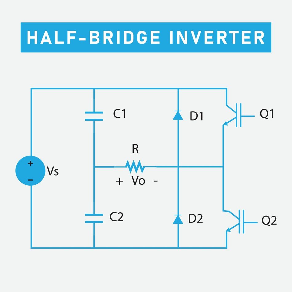
Operation with resistive and inductive loads: For a pure resistive load the output current has the same shape as the voltage. With an inductive load, the current lags and may reverse direction while the voltage is still positive.
Free‑wheeling diodes conduct when the load current is negative relative to the switch voltage, providing a path for energy and preventing voltage spikes.
Full‑bridge inverter (H‑bridge)
A full‑bridge inverter uses four switching devices arranged in an H‑bridge. Two diagonal switches conduct simultaneously to apply the full DC voltage across the load: switches (Q1, Q2) produce a positive voltage and switches (Q3, Q4) produce a negative voltage. The remaining two switches are off.
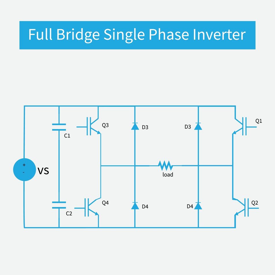
H‑bridge inverters offer double the output voltage compared with half‑bridge circuits and are prevalent in motor drives, solar power conditioning, and uninterruptible power supplies (UPS).
Suggested Reading: H Bridge Motor Control: A Complete Guide for Engineers 2025
Topology | Switches per phase | Output voltage levels | Fundamental RMS (resistive load) |
Half‑bridge | 2 switches + 2 diodes | ±V<sub>DC</sub>/2 | 0.45 V<sub>DC</sub> |
Full‑bridge | 4 switches + 4 diodes | ±V<sub>DC</sub> | 0.9 V<sub>DC</sub> |
Designers select switching devices based on power level, voltage rating, and efficiency. MOSFETs are favored for low‑voltage, high‑frequency operation; IGBTs are preferred for higher voltages and power levels. Free‑wheeling diodes enable bidirectional current flow.
When building a full‑bridge for a pure sine‑wave inverter, gate drivers such as the IR2110 provide the high‑side/low‑side drive signals; microcontrollers generate sinusoidal PWM, and an LC filter smooths the output to produce a clean sine wave.
Suggested Reading: Difference between Active and Passive Filters?
Modified Sine Wave Inverters
Some low‑cost inverters produce a modified sine wave: a stepped approximation to a sine wave with zero‑voltage intervals. Although cheaper than pure sine‑wave inverters, modified sine‑wave units have higher harmonic distortion and lower efficiency (75–85 %). They are not suitable for sensitive electronics or motors that require smooth torque.
Pulse‑width modulation and control strategies
Why PWM is necessary
Early inverters used simple square‑wave switching. The development of high‑frequency switching devices enabled pulse‑width modulation (PWM) to control the duty cycle and synthesise a near‑sinusoidal output. PWM offers several advantages:
Adjustable output voltage: The fundamental amplitude is proportional to the modulation index; by varying the duty cycle, the AC output voltage can be controlled without changing the DC input.
Reduced low‑order harmonics: Sinusoidal PWM suppresses low‑order harmonics, moving them to higher frequencies where filters are smaller and less costly.
Elimination of discrete voltage levels: PWM produces a smooth sinusoid after filtering rather than discrete steps.
The main drawback is the requirement for fast switching devices and sophisticated gate drivers. Switching losses increase with frequency, so designers must balance harmonic reduction against efficiency.
Sinusoidal PWM (SPWM)
The most common scheme is sinusoidal PWM. A sinusoidal reference signal is compared with a high‑frequency triangular carrier. When the sine wave exceeds the carrier, the comparator output goes high and turns on the upper switch; when it is below, the lower switch turns on. The resulting PWM pulses control the half‑bridge or full‑bridge, and the fundamental component of the output is proportional to the modulation index.
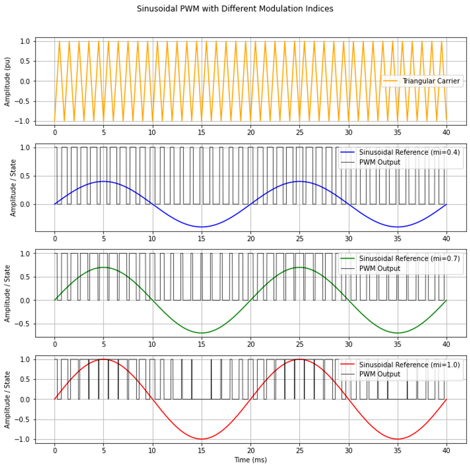
SPWM is easily implemented with microcontrollers or field‑programmable gate arrays (FPGAs). To produce three‑phase outputs, three sinusoidal references shifted by 120° are used.
Dead‑time and switching considerations
In both half‑bridge and full‑bridge configurations, two switches in the same leg mustn't turn on simultaneously; otherwise, the DC supply is shorted.
Designers insert a dead‑time (small delay between turning one switch off and the complementary switch on) to prevent cross‑conduction. Dead‑time introduces slight distortion because the output voltage remains at zero during the dead interval; careful timing and matched devices minimise distortion.
Further Reading: What Is a PWM Signal? Fundamentals and Practical Applications for Engineers
Filtering and Harmonic Mitigation
PWM inverters generate high‑frequency voltage steps that contain harmonics. LC filters are commonly placed at the output to attenuate switching harmonics and produce a clean sinusoidal waveform. The filter must be designed considering:
Cut‑off frequency: The filter’s resonant frequency should be well below the switching frequency but above the fundamental frequency.
Load impedance: The inductor and capacitor values must handle the expected current and voltage without saturating or experiencing large voltage swings.
Switching frequency: High modulation frequencies reduce the required inductance and capacitance, enabling smaller filters.
Filters also mitigate electromagnetic interference (EMI). A PV‑inverter white paper notes that PWM switching creates high di/dt and dv/dt noise; external LC filters and shielding are required to meet standards such as IEEE 1547 and UL 1741.
Suggested Reading: Low Pass Filter vs High Pass Filter – Theory, Design, and Applications
Efficiency Considerations
The efficiency of an inverter depends on conduction losses (due to the on‑resistance or saturation voltage of switching devices), switching losses (energy lost when turning devices on/off), and losses in magnetic components. Pure sine‑wave inverters typically achieve 90–95 % efficiency. Modified sine‑wave inverters operate at 75–85 % efficiency because the stepped waveform increases harmonic currents and heating.
Typical inverter efficiencies range from 85 % to 95 %, with pure sine‑wave units at the upper end and modified sine‑wave units at the lower end. Efficiency also varies with load; inverters have optimum efficiency near their rated power and degrade at light loads.
Three‑phase Inverter Circuits
Many industrial drives, EV traction systems and grid‑tied converters require three‑phase AC. A three‑phase inverter synthesises three sinusoidal voltages separated by 120°.
It uses six switching devices arranged in three legs. Each leg has an upper and lower switch; the upper switch conducts for part of the cycle, while the lower switch conducts during the complementary interval. Two common conduction modes define how long each switch remains on.
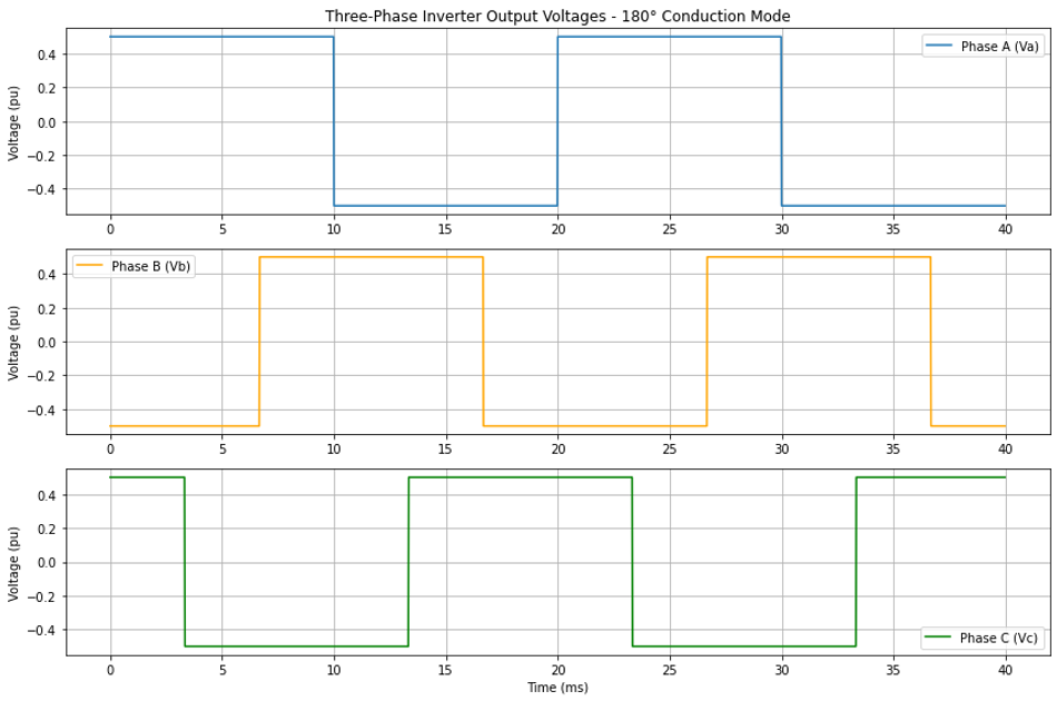
180° conduction mode
In the 180° conduction mode, each switch conducts for half of the fundamental cycle. At any given time three switches are on (one in each leg) and three are off. The switching intervals are shifted by 60° so that the phase voltages are balanced. For example, consider the first 60° interval (0°–60°): switches S1, S4 and S5 are on while the others are off. The resulting phase voltages are:

and the line voltages satisfy:

Other intervals follow a similar pattern as the switches cycle through their conduction periods. Key characteristics of the 180° mode include:
Maximum voltage utilisation: Because three switches conduct simultaneously, the DC source voltage is utilised more effectively.
Higher fundamental output voltage: Each phase sees a longer positive/negative cycle, resulting in a higher amplitude.
High power capability: The mode is suited to motor drives and high‑power conversion.
Fig 6: Output waveforms of a three-phase 180-degree conduction mode inverter
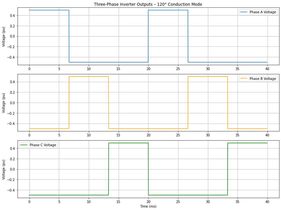
120° conduction mode
In the 120° conduction mode, each switch conducts for only 120° of the cycle. At any time two switches are on and one leg is floating. The switching sequence is similar but the conduction period is shorter; for instance, S1 conducts from 0°–120°, S3 from 120°–240° and S5 from 240°–360°. The shorter conduction reduces switching overlap and influences the voltage waveforms. Key characteristics include:
Reduced switching losses: Fewer devices are active simultaneously, so losses per device may be lower.
Different harmonic spectrum: The 120° mode produces a six‑step waveform with higher-order harmonics. The line voltages have segments where one phase is floating, resulting in lower voltage utilisation and different THD.
Simple control: Because each switch is on for 120°, the timing logic is straightforward.
When designing three‑phase inverters, engineers choose the conduction mode based on voltage utilisation, harmonic requirements, and control complexity. Most modern drives use PWM control with sinusoidal references for each phase rather than discrete 120°/180° conduction modes, but understanding these fundamentals aids troubleshooting and control design.
Circuit components and protection
A three‑phase inverter circuit employs components similar to the single‑phase case but replicated across three legs. Typically, inverters have the following components:
Six power switches: MOSFETs, IGBTs or thyristors arranged in three legs.
DC input source: Battery bank or rectified DC supply.
Protection diodes: Free‑wheeling diodes across each switch to clamp voltage and provide a current path during dead times and inductive load commutation.
Control circuit: Gate‑driver circuits or isolated drivers to generate accurate switching signals.
Filter components: Inductors and capacitors to smooth the output waveforms and meet THD limits.
Digital controllers such as microcontrollers or FPGAs generate the sinusoidal references and modulate each leg. Synchronisation of the three phase references ensures a balanced output. Protection mechanisms include over‑current sensors, thermal monitoring and isolation to avoid shoot‑through.
Suggested Reading: Circuit Board Components Identification: A Comprehensive Guide
Advanced Inverter Topologies
Multilevel inverters
As power levels increase and grid standards demand low harmonics, multilevel inverters (MLIs) have emerged. MLIs synthesize an output waveform with several discrete voltage levels using multiple DC sources or capacitors. Two popular topologies are the cascaded H‑bridge and flying capacitor inverters. Multilevel inverters offer several advantages:
Improved harmonic performance: The stepped output approximates a sine wave more closely, significantly reducing THD and electromagnetic interference (EMI).
Higher efficiency: Smaller voltage steps lower the voltage stress on switching devices and reduce switching losses. MLIs can achieve higher overall efficiency than two‑level inverters.
High output voltage with low voltage devices: By connecting multiple cells in series, MLIs generate high voltages without requiring devices with high blocking voltage. This reduces costs and enables modular construction.
MLIs are widely used in renewable‑energy systems (photovoltaic, wind), electric vehicle drivetrains, motor drives ,and HVDC transmission. Control schemes include level‑shifted PWM, phase‑shifted carrier PW,M and space vector modulation. Although MLIs require more components and complex control, the benefits often outweigh the additional cost in high‑power applications.
Wide‑bandgap Semiconductors (SiC and GaN)
Switching devices based on silicon carbide (SiC) and gallium nitride (GaN) offer faster switching, lower on‑resistance, and better thermal performance than traditional silicon MOSFETs or IGBTs. High‑frequency switching enabled by SiC/GaN reduces the size of filters and improves efficiency.
Modern switching devices such as SiC and GaN allow high switching frequencies and improve efficiency compared with silicon MOSFETs. Engineers designing next‑generation inverters should consider wide‑bandgap devices for high power density and high efficiency.
Suggested Reading: Where GaN can, it should, and GaN can in more and more places
Practical Design Considerations
Selecting switching devices
Choose MOSFETs or IGBTs based on voltage and power requirements. For low‑ to medium‑voltage applications (<200 V), MOSFETs with fast switching and low Rdson are appropriate. For higher voltages (>400 V) and high power, IGBTs provide lower conduction losses. When designing a pure sine‑wave inverter, pair the switches with a high‑side/low‑side gate driver (e.g., IR2110) to simplify gate drive and ensure proper dead‑time insertion.
Modulation Index and Output Control
In SPWM, the modulation index (ma)is the ratio of the peak of the reference sine wave to the peak of the triangular carrier. For a single‑phase full‑bridge inverter, the fundamental output voltage is proportional to ma. Keep ma ≤ 1 for linear modulation; over‑modulation (>1) produces a flat top and increases distortion. Microcontroller firmware should vary m<sub>a</sub> to achieve voltage regulation or implement closed‑loop control.
Cooling and thermal management
Switching devices dissipate heat during conduction and switching events. Provide heatsinks and forced‑air cooling to keep junction temperatures within safe limits. SiC and GaN devices allow higher temperature operation but still require thermal design. Over‑temperature sensors should trigger shutdown or throttling to protect the inverter.
EMI and layout
High dv/dt and di/dt transients in PWM inverters generate electromagnetic interference. Use short, wide traces for high‑current paths; place decoupling capacitors close to switching devices; and design PCB layouts to minimise loop areas. Shielding and proper grounding reduce radiated emissions.
LC filters should be physically separated from control circuitry to avoid noise coupling.
Safety and Isolation
Inverters connecting to the grid or driving AC loads must meet safety regulations. Provide galvanic isolation between the control electronics and high‑power stage using isolated gate drivers or transformers.
Electrical Glass Fuse Resistors Diode Transistor Stock Photo 1891512202 | Shutterstock
Implement over‑current protection (fuses, current sensors), over‑voltage clamps and soft‑start circuits. For grid‑tied systems, comply with standards such as IEEE 1547 for islanding protection, voltage and frequency limits, and THD requirements.
Conclusion
DC–to–AC inverters enable everything from portable power supplies to industrial motor drives. Understanding the underlying theory, topologies and control strategies empowers engineers to design efficient, reliable inverter systems. Half‑bridge and full‑bridge single‑phase circuits form the foundation, while pulse‑width modulation and LC filtering ensure clean sinusoidal outputs. Three‑phase inverters extend the concept using six devices with 120° or 180° conduction patterns to synthesize balanced three‑phase AC.
Advanced multi‑level inverters further reduce harmonics and enable high‑power, high‑voltage applications. When selecting switching devices, consider wide‑bandgap semiconductors for improved efficiency and compact filters. Proper thermal management, EMI suppression and safety measures are essential for robust designs. As renewable energy integration grows and power electronics continue to evolve, mastering inverter circuits remains a vital skill for engineers.
FAQs
1. What is the difference between a voltage‑source inverter and a current‑source inverter?
A voltage‑source inverter (VSI) has a low‑impedance DC input and synthesizes a controlled AC voltage output; it uses self‑commutating devices like MOSFETs or IGBTs. A current‑source inverter (CSI) has a high‑impedance DC source and produces a controlled AC current. CSIs typically use thyristors that require forced commutation and are used in high‑power drives.
2. Why is a full‑bridge inverter preferred over a half‑bridge inverter?
A full‑bridge inverter uses four switches to apply the full DC voltage across the load, providing a higher fundamental voltage (0.9 V<sub>DC</sub>) compared with 0.45 V<sub>DC</sub> for a half‑bridge. It does not require a center‑tapped DC source and offers better voltage utilisation. Consequently, full‑bridge inverters are common in motor drives, solar inverters and UPS systems.
3. How does sinusoidal PWM reduce harmonics?
Sinusoidal PWM compares a sinusoidal reference with a high‑frequency carrier. The duty cycle of the resulting pulses varies according to the sine wave, and the fundamental component of the output voltage is proportional to the modulation index. Low‑order harmonics are suppressed because the switching frequency is much higher; high‑order harmonics can be filtered with a modest LC network.
4. What is the purpose of dead‑time in inverter switching?
Dead‑time is a short delay inserted between turning off one switch and turning on its complementary switch in the same leg. It prevents both switches from conducting simultaneously, which would short the DC source and damage the devices. Dead‑time must be carefully calibrated to prevent shoot‑through while minimising distortion in the output waveform.
5. How do 180° and 120° conduction modes differ in three‑phase inverters?
In 180° conduction mode, each switch conducts for half of the fundamental cycle and three switches are on at any time. This maximises voltage utilisation and produces higher fundamental output voltage. In 120° conduction mode, each switch conducts for one‑third of the cycle; only two switches are on at any time, reducing switching overlap and losses but lowering the output voltage and altering the harmonic spectrum.
6. Why are multi‑level inverters used in high‑power applications?
Multi‑level inverters generate stepped output waveforms using multiple DC sources or capacitors. The increased number of voltage levels reduces harmonic distortion and voltage stress on devices, improving efficiency and power quality. MLIs enable high‑voltage outputs without requiring high‑voltage devices and are therefore popular in renewable‑energy interfaces, electric vehicles and HVDC systems.
7. Are pure sine‑wave inverters more efficient than modified sine‑wave inverters?
Yes. Pure sine‑wave inverters typically achieve 90–95 % efficiency, while modified sine‑wave inverters operate at 75–85 % efficiency. Modified sine‑wave inverters produce more harmonic currents, leading to greater losses and potential issues in sensitive loads. Pure sine‑wave inverters cost more but are recommended for most applications.
References
A. Asuri, "Single Phase Pulse Width Modulated Inverters," Tennessee Technological University, Cookeville, TN, USA. [Online]. Available: https://www.tntech.edu/engineering/pdf/cesr/ojo/asuri/Chapter2.pdf
Monolithic Power Systems, "Single Phase Inverters," MonolithicPower.com. [Online]. Available: https://www.monolithicpower.com/en/learning/mpscholar/power-electronics/dc-ac-converters/single-phase-inverters
Circuit Digest, "Three Phase Inverter Circuit Diagram - 120 Degree and 180 Degree Conduction Mode," CircuitDigest.com. [Online]. Available: https://circuitdigest.com/tutorial/three-phase-inverter-circuit-diagram-120-degree-and-180-degree-conduction-mode
M. R. Al-Mansoori et al., "Symmetry Applications for Greater Efficiency, Reliability, and Voltage Utilization in Grid-Connected Energy Systems," Symmetry, vol. 17, no. 7, 2025. [Online]. Available: https://www.mdpi.com/2073-8994/17/7/1010
Solectria Renewables, "Harmonics and Noise in Photovoltaic (PV) Inverter and the Impact on Power Quality," Solectria.com, White Paper. [Online]. Available: https://www.solectria.com/site/assets/files/1482/solectria_harmonics_noise_pv_inverters_white_paper.pdf
EcoFlow, "Pure Sine Wave Inverters: Complete Guide," EcoFlow.com, Sep. 2025. [Online]. Available: https://www.ecoflow.com/us/blog/pure-sine-wave-inverters-complete-guide
Linquip, "Efficiency of Inverter," Linquip.com. [Online]. Available: https://www.linquip.com/blog/efficiency-of-inverter
Microcontrollers Lab, "How to Make H-Bridge Using IR2110," MicrocontrollersLab.com. [Online]. Available: https://microcontrollerslab.com/how-to-make-h-bridge-using-ir2110
Power Electronics News, "Power Electronics Course Part 10: The Single-Phase Full Bridge Inverter," PowerElectronicsNews.com. [Online]. Available: https://www.powerelectronicsnews.com/power-electronics-course-part-10-the-single-phase-full-bridge-inverter/
Electrical Technology, "Half H Bridge Inverter: Its Modes of Operation with Waveforms," ElectricalTechnology.org. [Online]. Available: https://www.electricaltechnology.org/2020/06/half-h-bridge-inverter-its-modes-of-operation-with-waveforms.html
in this article
1. Introduction2. Fundamentals of DC–to–AC conversion3. Single‑phase inverter topologies4. Pulse‑width modulation and control strategies5. Filtering and Harmonic Mitigation6. Efficiency Considerations7. Three‑phase Inverter Circuits8. Advanced Inverter Topologies9. Practical Design Considerations10. Conclusion11. FAQs12. References