


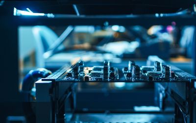
An Overview of the Different Edge AI Platforms.
Be the first to know.
Get our semiconductors weekly email digest.
Tagged with
semiconductors
ORGANIZATIONS. SHAPING THE INDUSTRY.
Nordic Semiconductor
Semiconductors
Nordic Semiconductor is a fabless semiconductor company specializing in wireless technology that powers the IoT.
181 Posts

Intrinsic ID
Semiconductor
Securing the IoT with the World's Top PUF Technology. Authenticate Everythi...
16 Posts
Latest Posts


Benefits, Utilities, and Hybrid Deployment of Edge AI.

How Edge AI is Transforming Industries and Application Areas.

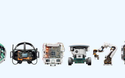
The guide to understanding the state of the art in hardware & software in Edge AI.
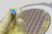
Integrated photonics, also known as planar lightwave circuits or integrated optical circuits, revolutionizes optical communication by leveraging the properties of light to process and transmit information. This cutting-edge technology offers superior efficiency and compactness compared to traditional electronic components, paving the way for faster and more energy-efficient communication systems. With its interdisciplinary nature encompassing materials science, quantum physics, and electrical engineering, integrated photonics presents an exciting and promising field of study and research in today's digital era.
Advanced testing methodologies and innovation in semiconductor packaging ensure product reliability in dynamic and harsh operational environments. These strategies are particularly crucial in the rapidly evolving automotive industry.

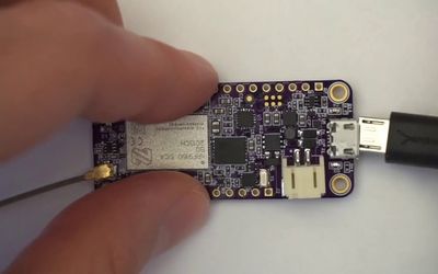
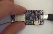
A guide to resources related to the Nordic Semiconductor nRF9160 Development Kit and Soracom connectivity to help you launch your Connect For Good Low Power Wireless Sustainability Challenge submission.
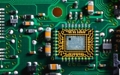
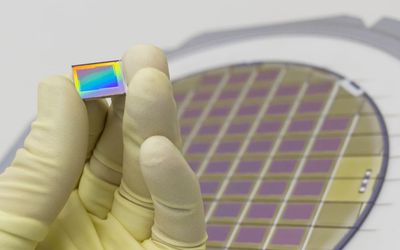
Silicon, with its abundant availability and unique properties, serves as the fundamental building block for semiconductor manufacturing. Its semi-metallic nature makes it an ideal material for controlled conduction of electricity. Furthermore, the combination of silicon with oxygen produces silicon dioxide, a crucial insulating component in silicon chip manufacturing.
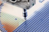
Die attach, also known as die bonding or die mount, is a process used in the semiconductor industry to attach a silicon chip to the die pad of a semiconductor package's support structure, such as a leadframe or metal can header. This article explores the fundamentals of die attach, its importance, materials, and methods used in die attach, its parameters, quality, and reliability techniques.
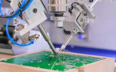
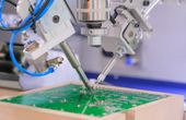
Soldering Unveiled: Exploring Wave and Reflow Techniques for Engineering Graduates. Delve into the Depths of PCB Assembly, Component Compatibility, Production Efficiency, and Quality Assurance. Gain Profound Insights into Wave Soldering Machines, Reflow Ovens, and the Art of Soldering. Empower Your Engineering Journey with this In-Depth Comparative Analysis of Two Key Soldering Methods.
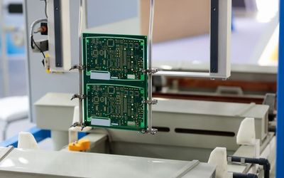
This guide dives deep into the world of PCB surface finishes: In this article, you will experience a comprehensive analysis of various types, factors for optimal performance, and comparing different PCB finishes to choose right one for your specific application
Understanding Plasma Etching: Detailed Insights into Its Techniques, Uses, and Equipment Maintenance
Plasma etching is a salient process in various engineering fields, especially in electronics and materials science. It's a method used to etch or carve fine patterns on the surface of substrates, such as silicon wafers used in semiconductor manufacturing. It works by creating a plasma or ionized gas within a chamber, which chemically reacts with the material on the substrate's surface, effectively removing it. Plasma etching is highly precise and allows for the creation of extremely intricate patterns at a microscopic level.
Ion milling is a material etching technique used extensively in modern manufacturing and research. It involves the bombardment of a sample with charged particles, called ions, to remove material from the surface in a controlled manner. This article explores the fundamental principles of ion milling, the various techniques used, the equipment required, and its applications in different fields.
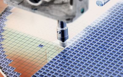
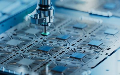
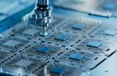
Wafer dicing separates individual integrated circuits or chips from a semiconductor wafer without damaging their delicate structures and circuits. This process is crucial for the production of electronic devices and components used in various industries, and the demand for it has increased with the development of high-performance and smaller electronic devices. Different dicing techniques, such as blade dicing, laser dicing, and plasma dicing, have been developed, and new innovations continue to emerge to address the challenges of complex semiconductor devices.
An Overview of Magnetron Sputtering and its Applications in Thin Film Growth