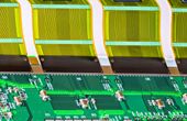
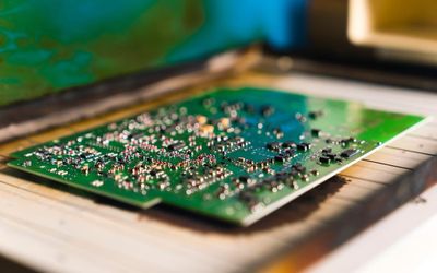
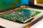
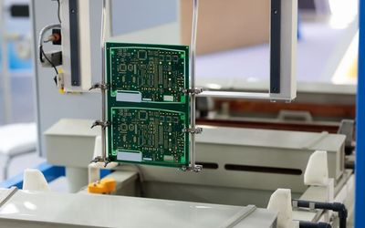
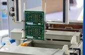
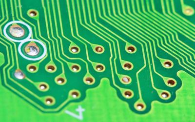
This article provides a detailed overview of the solder reflow process, types of reflow ovens, temperature profiles, solder paste composition and selection, reflow process potential challenges, solutions, inspection, and quality control techniques.
Be the first to know.
Get our pcb weekly email digest.
Tagged with
PCB
ORGANIZATIONS. SHAPING THE INDUSTRY.


HQ NextPCB
Appliances, Electrical, and Electronics Manufacturing
HQ NextPCB specializes in reliable multilayer PCB manufacture and assembly ...
1 Post

AllSpice
Software Development
Hardware collaboration platform 🤖 Inspired by software development princip...

Latest Posts
This guide dives deep into the world of PCB surface finishes: In this article, you will experience a comprehensive analysis of various types, factors for optimal performance, and comparing different PCB finishes to choose right one for your specific application
Surface profile is vital for material performance across industries. A deep understanding of it will help engineers optimize material properties, enhance product performance, and ensure component durability. This article explores its fundamentals, significance, and diverse applications.

Understanding Plasma Etching: Detailed Insights into Its Techniques, Uses, and Equipment Maintenance
Plasma etching is a salient process in various engineering fields, especially in electronics and materials science. It's a method used to etch or carve fine patterns on the surface of substrates, such as silicon wafers used in semiconductor manufacturing. It works by creating a plasma or ionized gas within a chamber, which chemically reacts with the material on the substrate's surface, effectively removing it. Plasma etching is highly precise and allows for the creation of extremely intricate patterns at a microscopic level.

Printed Circuit Boards (PCBs) are an essential component of nearly every electronic device, providing the foundation for the connections and features that enable functionality. As technology advances and devices become more complex, the importance of efficient and effective PCB layout design has become increasingly critical. This article will guide you through designing a PCB layout, from understanding the basics to mastering advanced techniques and preparing for manufacturing.
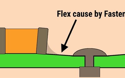
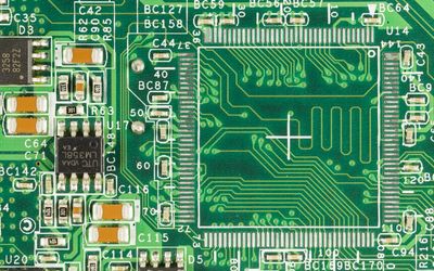
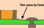
Picking the right fastener can be tricky.

4 minutes read
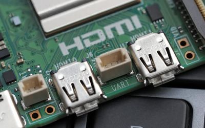
UART and SPI are key communication methods in electronics. UART is ideal for simple, long-distance connections, while SPI excels in fast data transfer. Used in GPS modules, SD cards, and microcontrollers, understanding their differences can help you choose the best for any given project.

Thermal analysis can identify key areas of temperature risk. Learn design strategies for coping with and dissipating excess heat.
2 minutes read

The purpose of this article is to provide a comprehensive, in-depth guide to PCB soldermask, exploring the key concepts, principles, and practical applications that will help you excel in PCB design and manufacturing.

New fabs will focus on making cutting-edge chips, not those based on older, established technology. So how should your company solve for potential limited supplies?
4 minutes read

Discover what tented vias are in PCB design and how to use them effectively – covering their definition, benefits, drawbacks, and best practices from design through manufacturing!

Find out the drivers and challenges that are facing the industrial robotics industry
3 minutes read

Castellated holes are extensively used in the printed circuit board (PCB) design process. This article is a detailed overview of castellated holes, covering their history, application, benefits, design attributes, challenges, and significance in modern electronic design.
Many companies are now looking at alternatives to silicon chips.
5 minutes read
Find out why rigid-flex PCB assembly has become increasingly popular in modern electronic production.
3 minutes read