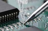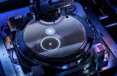
As electronics become smaller and more powerful, heat dissipation has become a major concern.

8 minutes read
Tagged with


Appliances, Electrical, and Electronics Manufacturing
HQ NextPCB specializes in reliable multilayer PCB manufacture and assembly ...
1 Post

Software Development
Hardware collaboration platform 🤖 Inspired by software development princip...

As electronics become smaller and more powerful, heat dissipation has become a major concern.
8 minutes read
Building open communication within internal teams is the first hurdle.
6 minutes read
Fostering a culture of continuous improvement encourages team members to contribute ideas and solutions that lead to better products.
Despite the prevalence of newer surface mount technology, THT still retains several unique benefits that underscore its enduring relevance. Find out which method is best for your projects.
10 minutes read
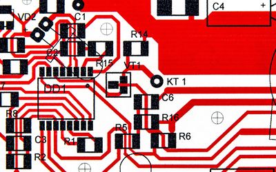
Castellation PCB is a type of printed circuit board (PCB) that has a series of small, plated through holes along the edges of the board. These holes are used to create a connection between the board and other components in a circuit. This article delves into the design, manufacturing, and testing processes involved in creating castellation PCBs, providing insights into the key considerations and guidelines that engineers and manufacturers should follow to optimize their designs for performance, reliability, and manufacturability.
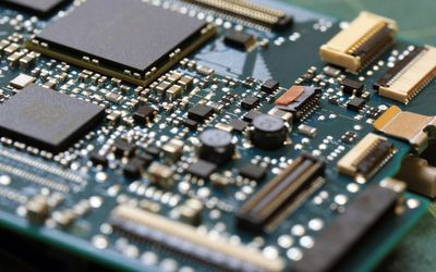
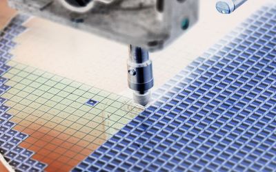
Semiconductors are the building blocks of modern electronics, powering everything from smartphones to satellites. This in-depth guide provides a comprehensive understanding of semiconductors' engineering principles and applications, delving into their fundamental concepts, materials, devices, manufacturing processes, and their impact on today's technology landscape.
Companies with strong ESG performance reduce costs by 5 to 10 percent.
7 minutes read
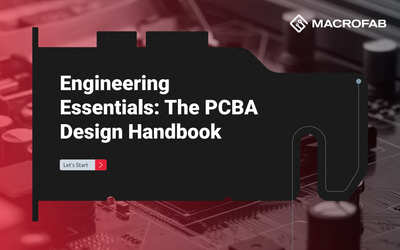
This 75-page e-book will provide you with the design skills to develop exceptional PCBAs that not only meet but surpass their intended objectives.
4 minutes read
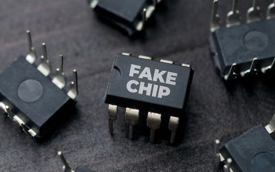
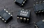
There is a real and growing threat of counterfeit products within the electronics industry. Do you know how to mitigate it?
6 minutes read
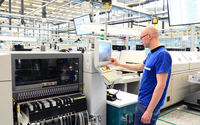
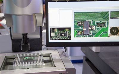
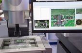
2D and 3D Automated inspection systems are often used for detecting manufacturing errors in fast production lines. Learn how they provide a comprehensive and efficient solution for quality assurance.
With the increasing need for critical applications technology, PCBAs have become smaller and more complex, requiring designers to create more individual designs in a shorter timeframe. Learn how to do so while avoiding common errors that can derail your project.
8 minutes read
Fifteen percent of electronic parts disappear from the market annually. Are you ready if one of them is part of your design?
5 minutes read
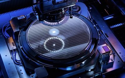
Silicon, with its abundant availability and unique properties, serves as the fundamental building block for semiconductor manufacturing. Its semi-metallic nature makes it an ideal material for controlled conduction of electricity. Furthermore, the combination of silicon with oxygen produces silicon dioxide, a crucial insulating component in silicon chip manufacturing.
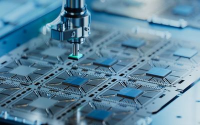
Die attach, also known as die bonding or die mount, is a process used in the semiconductor industry to attach a silicon chip to the die pad of a semiconductor package's support structure, such as a leadframe or metal can header. This article explores the fundamentals of die attach, its importance, materials, and methods used in die attach, its parameters, quality, and reliability techniques.
Fifteen percent of electronic parts disappear from the market annually. Are you ready if one of them affects your design?
5 minutes read