Half Adder vs Full Adder: Comprehensive Guide for Engineers
This in depth article compares halfadders and fulladders, the core building blocks of digital circuits. It explains their theory, truth tables, logical expressions, practical implementations and performance tradeoffs. Learn how to implement these adders in hardware description language.

22 Dec, 2025. 11 minutes read

Key Takeaways
A half adder adds two single‑bit numbers and outputs the sum and carry; a full adder adds three bits (including carry‑in).
Half adders have two inputs (A, B) and two outputs (Sum, Carry); full adders have three inputs (A, B, Cin) and two outputs (Sum, Cout).
A half adder uses one XOR gate and one AND gate; a full adder typically uses two XOR gates, two AND gates and one OR gate.
Half adders are ideal for simple binary addition without a carry‑in (e.g., LSB addition). Full adders are essential for multi‑bit addition in processors, as are ripple-carry adders.
Full adders can be constructed from two half adders and an OR gate, making half adders foundational components of more complex adder structures.
Introduction
Digital electronics is based on binary addition. It is the backbone of modern computing. Whether you are designing a simple arithmetic logic unit (ALU) or a sophisticated processor, understanding the mechanisms that perform addition is crucial. Half adders vs full adders is a classic topic in digital design because these circuits form the basis of arithmetic operations.
This article will delve into their theoretical underpinnings, differences in logic, truth tables, and Boolean expressions, and how to implement them in practice. We will also discuss performance considerations, HDL coding examples, real‑world applications, and advanced design techniques.
By the end of this article, you will have a thorough grasp of half adders and full adders, enabling you to design optimized circuits.
The Importance of Digital Addition
Why Binary Addition Matters
Digital systems use binary numbers to represent data and perform arithmetic operations. The simplest operation—binary addition—requires adding two bits and handling any carry that results.
As systems scale from single‑bit to multi‑bit computations, adders become essential building blocks in ALUs, multipliers, and addressing units. Efficient adder design influences the speed and power consumption of processors, making it a key area of optimization.
The Hierarchy of Adders
Half Adder (HA): Adds two single bits (A and B). Outputs sum (S) and carry (C). It does not handle a carry‑in from a previous stage.
Full Adder (FA): Adds three bits (A, B, Cin). Outputs sum (S) and carry‑out (Cout). It accounts for a carry‑in from a previous addition.
Ripple‑Carry Adder (RCA): Cascades multiple full adders (with one half adder at LSB if needed) to add multi‑bit numbers.
Look‑ahead and Tree Adders: Advanced designs (e.g., carry‑look ahead, carry‑save, Wallace tree, Dadda tree) improve speed by reducing carry propagation delay.
What are Half Adders?
A half adder is a combinational circuit that adds two single‑bit binary numbers, A and B. It outputs two bits: the sum (S) and the carry (C). The Boolean logic of a half adder is:
Sum: S = A ⊕ B
Carry: C = A . B
Here is the truth table for the expressions:
| A | B | S | C |
| 0 | 0 | 0 | 0 |
| 0 | 1 | 1 | 0 |
| 1 | 0 | 1 | 0 |
| 1 | 1 | 0 | 1 |
Logic Gates Used
XOR gate: Produces the sum.
AND gate: Produces the carry.
Half adders are used for operations where there is no incoming carry, such as adding the least significant bits of two binary numbers.
Further Reading: Half Adder Circuit—Theory, Design, and Implementation
Full Adder Fundamentals
A full adder is a combinational circuit that adds three bits—A, B, and Cin (carry‑in)—and outputs a sum bit (S) and a carry‑out bit (Cout). The boolean expressions are:
Sum: S = A ⊕ B ⊕ Cin
Carry‑out: Cout = A.B ⊕ ACin ⊕ BCin
These formulas derive from simplifications of the full adder truth table and Karnaugh‑map reduction. The truth table is:
| A | B | Cin | Sum | Cout |
| 0 | 0 | 0 | 0 | 0 |
| 0 | 0 | 1 | 1 | 0 |
| 0 | 1 | 0 | 1 | 0 |
| 0 | 1 | 1 | 0 | 1 |
| 1 | 0 | 0 | 1 | 0 |
| 1 | 0 | 1 | 0 | 1 |
| 1 | 1 | 0 | 0 | 1 |
| 1 | 1 | 1 | 1 | 1 |
Logic Gates Used
Standard full adder implementations use:
Two XOR gates
Two AND gates
One OR gate.
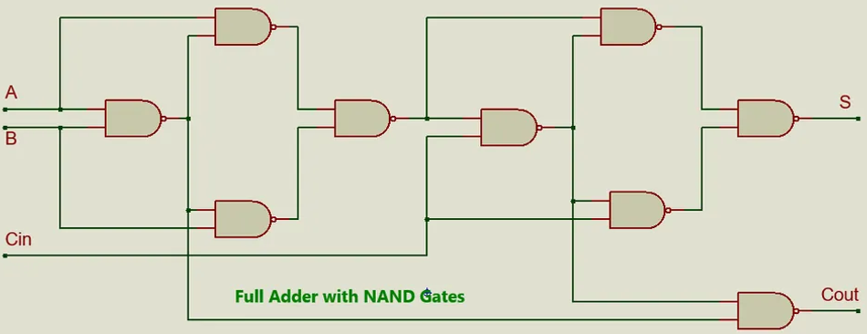
However, a full adder can also be built using nine NAND gates or nine NOR gates due to gate completeness. Understanding these alternatives allows for design flexibility when constrained to specific gate types.
Further Reading: Full Adder Circuit: Theory, Design and Practical Implementation
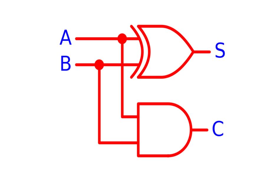
Relationship Between Half and Full Adders
A full adder can be constructed using two half adders and one OR gate. Connect A and B to the first half adder; then feed its sum output and Cin into the second half adder. OR the carry outputs of both half adders to produce the final Cout.
This modular design underscores the fact that half adders are the basic building blocks for full adders.
Adder Circuit Implementation with Logic Gates
Half Adder Circuits
Half adders can be implemented using the XOR gate for the sum, and an AND gate for the carry output. These are relatively straightforward and can be built using many digital logic families, such as 74HCxx, and many others. Typically, these families are most suited for prototyping applications.
Full Adder Circuits
There are multiple approaches to creating a full adder circuit. Firstly, a full adder may be implemented using two XOR gates to calculate the sum. Additionally, a combination of AND and OR gates can calculate the carry.
Moreover, full adders can be created using two half adder circuits and an additional OR gate. These techniques are more suited for demonstration and teaching the fundamentals of adder circuits.
Secondly, full adders can be implemented using the universal gates, i.e., NAND and NOR gates. It reduces the dependency on other logic gates and is easier to implement in hardware as one integrated circuit can have multiple logic gates. So, it reduces hardware complexity.
Hardware Description Languages (HDL)
Adder circuits can be implemented in FPGA designs via Hardware Descriptive Languages (HDL).
Typically, Verilog and VHDL are most commonly used for the implementation of these logic circuits through coding techniques.
Implementing Half Adder with HDL
The following table shows the examples of implementing Half Adders through VHDL and Verilog.
| VHDL Code | Verilog Code |
library IEEE;
use IEEE.STD_LOGIC_1164.ALL;


entity half_adder is
    Port ( A  : in  STD_LOGIC;
           B  : in  STD_LOGIC;
           S  : out STD_LOGIC;
           C  : out STD_LOGIC);
end half_adder;
architecture Behavioral of half_adder is begin S <= A xor B; C <= A and B; end Behavioral; | module half_adder ( input A, B, output S, C ); assign S = A ^ B; assign C = A & B; endmodule |
By using the structural design, a half adder can be reused to create full adders. Moreover, both examples allow the synthesis of adder circuits into FPGAs and ASICs.
Implementing a Full Adder with HDL
Implementing full adders becomes even easier as they can be synthesized using the half adder modules. The following table shows the examples of implementing Full Adders through VHDL and Verilog:
| VHDL Code | Verilog Code |
library IEEE; use IEEE.STD_LOGIC_1164.ALL; entity full_adder is Port ( A : in STD_LOGIC; B : in STD_LOGIC; Cin : in STD_LOGIC; S : out STD_LOGIC; Cout: out STD_LOGIC); end full_adder; architecture Structural of full_adder is signal S1, C1, C2: STD_LOGIC; component half_adder Port ( A, B : in STD_LOGIC; S, C : out STD_LOGIC); end component; begin HA1: half_adder port map (A => A, B => B, S => S1, C => C1); HA2: half_adder port map (A => S1, B => Cin, S => S, C => C2); Cout <= C1 or C2; end Structural; | module full_adder ( input A, B, Cin, output S, Cout ); wire S1, C1, C2; half_adder HA1 (.A(A), .B(B), .S(S1), .C(C1)); half_adder HA2 (.A(S1), .B(Cin), .S(S), .C(C2)); assign Cout = C1 | C2; endmodule |
Suggested Reading: FPGA Programming: Theory, Workflow, and Practical Implementations
Integrated Circuit (IC) Implementations
Half Adder IC: While there is no dedicated single IC marketed exclusively as a “half adder,” typical implementation uses ICs like SN74HC86 (XOR) and SN74HC08 (AND) from the 74HCxx series.
Full Adder IC: The 74LS83 is a classic four‑bit binary full adder with fast TTL logic. For modern designs, FPGAs or ASIC libraries provide parameterized adders with optimized gate counts.
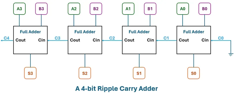
Building Multi‑Bit Adders
To add two 8‑bit numbers, you cascade eight full adders; the first stage can be replaced by a half adder if the initial carry‑in is zero. The carry‑out from one stage becomes the carry‑in to the next.
This structure is known as a ripple‑carry adder. It is simple but slow because each stage must wait for the carry from the previous stage. Engineers often replace ripple‑carry adders with faster designs like carry-look-ahead or carry‑select adders when performance is critical.
Comparative Analysis
Differences Between Half Adder and Full Adder
The following table highlights the primary differences, using insights from multiple sources.
Parameter | Half Adder | Full Adder |
Definition | Adds two single‑bit numbers | Adds two single‑bit numbers plus a carry‑in |
Inputs | A, B | A, B, Cin |
Outputs | Sum, Carry | Sum, Carry‑out |
Carry Handling | Does not accept carry‑in | Accepts carry‑in from previous stage |
Logic Gates | 1 XOR + 1 AND | 2 XOR + 2 AND + 1 OR |
Complexity | Simple | More complex |
Use Cases | Addition of least significant bits, simple binary addition | Multi‑bit addition, ALUs, ripple‑carry adders |
Replacement | Cannot replace a full adder | Can replace a half adder |
Design Trade‑Offs
Gate Delay: Full adders have greater logic depth; each carry must propagate through at least two gate levels (XOR/AND and OR). Half adders have fewer gates and thus lower delay, but they lack carry‑in handling.
Power Consumption: More gates in full adders lead to higher power usage. In low‑power designs (e.g., embedded systems), designers may use adder architectures that minimize active gates.
Area: On FPGAs or ASICs, half adders consume fewer logic resources. However, using separate half adders for each bit would require additional logic for carry propagation, negating area savings.
Flexibility: Full adders are versatile because they handle carry propagation. In multi‑bit addition, a full adder can always replace a half adder; the reverse is not true.
Applications of Adder Circuits
The following table summarizes the applications of these adder circuits.
Half Adder | Full Adder |
Used in simple arithmetic operations like half‑word addition. | Used in ripple‑carry, carry‑look ahead, carry‑select, and carry‑save adders. |
These are the building blocks for constructing full adders. | Full adders are the core of binary addition in ALUs, CPU arithmetic units. |
Used in digital calculators and microcontrollers, where initial bit addition occurs without incoming carry. | These are essential for multipliers (e.g., Wallace and Dadda multipliers) where partial products are reduced using full and half adders. |
These are ideal for educational tools for understanding logic circuits. | Implemented in custom ASICs, FPGAs and integrated circuits for low‑level arithmetic. |
Performance Considerations
Delay and Propagation
In ripple‑carry adders, each full adder must wait for the carry‑out from the previous stage. If a 32‑bit ripple‑carry adder uses full adders with a gate delay of tg, the worst‑case delay is roughly ( 2n + 1 ) gate delays (for n bits), because each carry can require two gate levels plus an initial XOR for the sum. For a 32‑bit adder, this results in 65 gate delays.
To mitigate this delay:
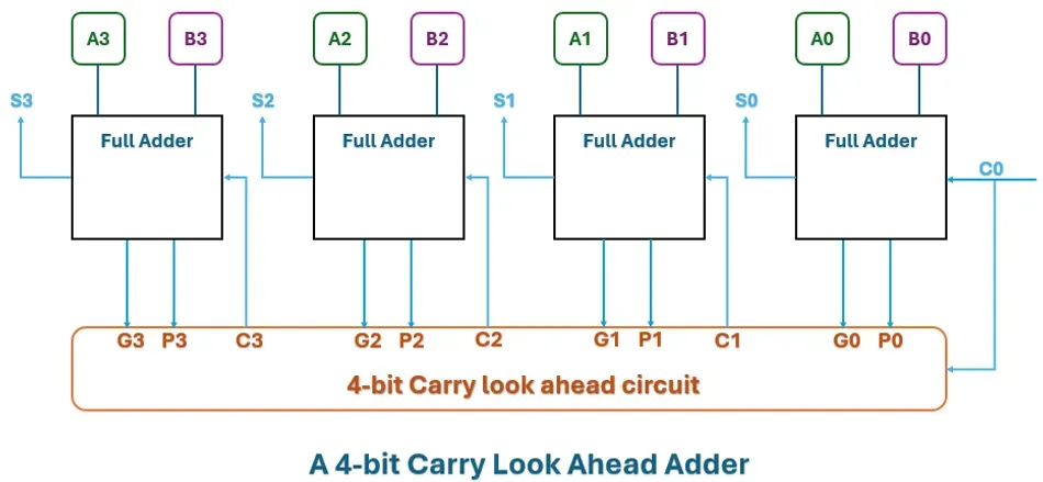
Carry‑Look Ahead Adders (CLA): Compute carries in parallel using generate and propagate signals.
Carry‑Save Adders (CSA): Use multiple adders to compute partial sums without immediate carry propagation; used in multipliers.
Carry‑Select Adders (CSL): Precompute results for both possible carry‑in values and multiplex the correct output.
These advanced structures are built on the same principles of half adders and full adders, yet reduce propagation delay significantly.
Power and Area Optimization
Designers often minimize switching activity to reduce dynamic power. In ASICs, full adder cells can be optimized using transistor‑level design (e.g., complementary CMOS logic, transmission gates) to reduce power while meeting timing constraints.
For FPGAs, LUT (look‑up table) based adders can map multiple logic functions into a single LUT, reducing area.
Practical Examples and Case Studies
Case Study 1: Building a 4‑Bit Adder Using Verilog
Below is a simple example of a 4‑bit ripple‑carry adder using four full adders (the first can be replaced by a half adder since the initial carry‑in is zero):
module ripple_adder_4bit (
    input [3:0] A,
    input [3:0] B,
    output [3:0] Sum,
    output Cout
);
wire c1, c2, c3;


half_adder HA0 (.A(A[0]), .B(B[0]), .S(Sum[0]), .C(c1));
full_adder FA1 (.A(A[1]), .B(B[1]), .Cin(c1), .S(Sum[1]), .Cout(c2));
full_adder FA2 (.A(A[2]), .B(B[2]), .Cin(c2), .S(Sum[2]), .Cout(c3));
full_adder FA3 (.A(A[3]), .B(B[3]), .Cin(c3), .S(Sum[3]), .Cout(Cout));
endmodule
This adder can be synthesized onto an FPGA board. However, for higher bit widths, the ripple delay becomes significant, encouraging designers to use more advanced adders.
Suggested Reading: Comprehensive Guide to 4-bit Adders: Theory, Implementation and Modern Innovations
Case Study 2: Implementing Full Adder Using Half Adders on a Breadboard
Place two XOR gates and two AND gates on the breadboard.
Connect inputs A and B to the first half adder (XOR and AND).
Feed the sum output (S1) of the first half adder and Cin to the second XOR gate (to produce the final sum).
Use the AND gate for S1 and Cin to produce the second carry (C2).
OR (or XOR if using the simplified expression) the carries C1 and C2 to produce Cout.
Test using switches and LEDs to verify truth table outputs.
Such physical implementation helps students grasp the circuit operation.
Case Study 3: Dadda Multiplier
In a Dadda multiplier, multiple partial products are summed using a combination of half and full adders arranged in a reduction tree. Each stage compresses the number of bits in each column until only two rows remain, which are then added using a conventional adder.
Full adders handle columns with three bits; half adders handle columns with two bits. Understanding half adders and full adders is thus essential for grasping the multiplier's architecture.
Advanced Topics
Optimized Full Adders
Researchers have developed optimized full adder circuits that minimize power, delay and transistor count. For example, XOR–XNOR based full adders combine exclusive OR and exclusive NOR gates to reduce transistor count, while mirror adder designs maintain balanced rise/fall times.
In deep submicron technologies, threshold voltage variation and leakage become critical; thus, designing full adders with transmission gates or dynamic logic may yield efficiency.
Adder in Arithmetic Logic Units (ALUs)
In microprocessors, the ALU typically includes adders that can add, subtract, and perform logic operations. Full adders are used in arithmetic operations and sometimes combined with logic for two’s complement arithmetic, enabling subtraction by adding a number’s two’s complement.
For high-performance processors, designers often employ carry-look-ahead adders or Kogge-Stone adders to achieve faster performance.
Quantum and Reversible Adders
Emerging computing paradigms explore quantum adders and reversible logic adders. Reversible adders, such as the Peres or Toffoli adder, ensure that no information is lost during computation, which theoretically allows for zero energy dissipation.
Quantum full adders use qubits and gates like CNOT and Toffoli to perform addition in quantum circuits.
Suggested Reading: The Role Of Quantum Computing In Manufacturing
Conclusion
Half adders and full adders are fundamental components in digital circuit design. A half adder adds two single‑bit numbers and produces the sum and carry, making it suitable for initial bit addition. A full adder extends this functionality by incorporating an incoming carry, enabling multi‑bit binary addition. Understanding their Boolean expressions, truth tables, and gate implementations is crucial for designing efficient arithmetic circuits.
In practical applications, full adders are the backbone of processors, ALUs, multipliers, and addressing units. By combining half adders, designers can construct full adders and ripple‑carry adders. However, performance constraints in modern systems lead to advanced adder architectures like carry‑look ahead, carry‑select, carry‑save, and adder trees, which still rely on the principles introduced here.
As you design digital circuits, keep the trade‑offs between simplicity, speed, and power in mind. Choosing the right type of adder and optimizing its implementation will improve the overall performance of your system.
FAQs
1. What is the main difference between a half adder and a full adder?
A half adder adds two single‑bit binary numbers and generates sum and carry without considering a previous carry. A full adder adds two single‑bit numbers and a carry‑in, producing sum and carry‑out.
2. Why can a full adder replace a half adder but not vice versa?
A full adder handles an additional carry‑in input. In multi‑bit addition, the least significant bit usually doesn’t have a carry‑in, so a half adder can suffice. However, if you only have full adders, you can set the carry‑in to zero for the first stage, effectively performing the same operation as a half adder.
3. How can I implement a full adder using half adders?
Use two half adders: feed inputs A and B into the first; take its sum and Cin into the second; OR the carry outputs to produce Cout. This modular implementation is common in textbooks and HDL examples.
4. What are typical applications of half adders?
Half adders are used for adding the least significant bits of binary numbers, in simple arithmetic operations, digital counters and as building blocks for full adders. They’re also useful in teaching logic design principles.
5. Which HDL is better for designing adders: VHDL or Verilog?
Both VHDL and Verilog can describe combinational circuits effectively. Verilog has a C‑like syntax and is popular in the U.S., while VHDL is more verbose and strongly typed, favored in Europe and for safety‑critical systems. Choose based on project requirements and team expertise.
6. What is the maximum bit width for which a ripple‑carry adder is practical?
For small bit widths (e.g., 8–16 bits) and non‑critical performance requirements, ripple‑carry adders are practical due to their simplicity. For larger bit widths (32 bits or more) or high‑frequency designs, carry‑look ahead or other fast adders are preferred to reduce propagation delays.
7. Can adders be used for subtraction?
Yes. Subtraction can be performed by adding the two’s complement of the subtrahend. This involves inverting the bits of the subtrahend and adding one via the carry‑in input of a full adder chain.
References
GeeksforGeeks—Difference between Half Adder and Full Adder, available at: https://www.geeksforgeeks.org/gate/difference-between-half-adder-and-full-adder/
TutorialsPoint—Difference between Half Adder and Full Adder, available at: https://www.tutorialspoint.com/digital-electronics/difference-between-half-adder-and-full-adder.htm
GeeksforGeeks—Implementation of Full Adder Using Half Adders, available at: https://www.geeksforgeeks.org/digital-logic/implementation-of-full-adder-using-half-adders
Electronics For You—Half Adder and Full Adder, available at: https://www.electronicsforu.com/technology-trends/learn-electronics/half-adder-full-adder-truth-table-circuit-working-kmap
Wikipedia—Adder (electronics), available at: https://en.wikipedia.org/wiki/Adder