What is an ASIC: A Comprehensive Guide to Understanding Application-Specific Integrated Circuits
This article provides an in-depth exploration of the evolution, fundamental concepts, diverse types, operating principles, and practical applications of ASICs.

01 Mar, 2024. 16 minutes read
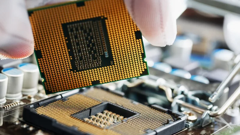
CPU Motherboard Component as ASIC
Introduction to ASICs
What is an ASIC? An Application-Specific Integrated Circuit (ASIC) is a specialized integrated circuit (IC) designed for specific applications instead of general-purpose use. ASICs differ fundamentally from general integrated circuits like microprocessors and memory chips, designed for diverse applications and mass production. They are typically used in all electronics, from cars and planes to smartphones and home appliances.
The primary objective of ASICs is to achieve a specific functionality with the highest possible efficiency. This efficiency can be in terms of power consumption, performance, cost, or a combination of these factors. By designing an ASIC to perform a specific function, it is possible to optimize its design to achieve the best possible performance for that function. This targeted approach often results in significant efficiency gains compared to using a general-purpose IC for the same function.
For example, in cryptocurrency mining, ASICs have been designed to perform the specific computations required for mining certain cryptocurrencies. These ASICs can perform these computations much more efficiently than a general-purpose computer, resulting in a significant increase in mining performance.
Still wondering what is an ASIC? This article provides an in-depth exploration of the evolution, fundamental concepts, diverse types, operating principles, and practical applications of ASICs.
The Evolution of ASICs
In the early days, integrated circuits were not application-specific. They were general-purpose chips that could be used in a variety of applications. However, as the demand for more precise and efficient electronic devices grew, the need for specialized integrated circuits became apparent. This led to the development of ASICs, designed to perform a specific function in an electronic device.
The development of ASIC technology was driven by the increasing complexity of electronic devices and the need for more efficient and powerful chips. Over the years, ASICs have become more complex and powerful, with modern ASICs containing millions of transistors.
The evolution of ASICs has been marked by continuous improvement and innovation. Each new generation of ASICs has brought significant improvements in terms of performance, power efficiency, and cost-effectiveness. This has made ASICs an integral part of modern electronic devices and systems.
Early Beginnings
The early beginnings of ASIC technology can be traced back to the 1960s. At this time, the electronics industry was dominated by general-purpose integrated circuits. These were versatile ASIC chips that could be used in various applications. However, they were not particularly efficient or powerful.
The need for more efficient and powerful chips led to the development of ASICs. These were specialized chips that were designed to perform a specific function. The first ASICs were relatively simple, with a limited number of transistors. However, they represented a significant leap forward in terms of efficiency and performance.
The development of ASIC technology was driven by the increasing complexity of electronic devices. As devices became more complex, the need for more efficient and powerful chips became apparent. This led to the development of more advanced ASICs capable of performing more complex functions.
The early ASICs were used in a variety of applications, from telecommunications to consumer electronics. They played a crucial role in the development of the electronics industry, enabling the creation of more sophisticated and efficient devices. Robert Lipp created the first CMOS array in 1974, but viable CAD support was not forthcoming for several years. VLSI Technology and LSI Logic in 1980s used these CAD-based ASIC concepts due to lower computing costs. [1]
Over the years, ASIC technology has evolved significantly. Modern ASICs are far more powerful and complex than their early counterparts, with millions of transistors. Despite these advancements, the basic principle of ASIC technology remains the same: to provide a highly efficient and powerful solution for a specific application.
Modern ASICs
The modern era of ASICs, which began in the late 1990s and continues to this day, has seen a dramatic increase in the complexity and capabilities of these specialized chips. Today's ASICs are vastly more powerful than their predecessors, capable of highly complex tasks with incredible efficiency.
One of the key factors driving the evolution of modern ASICs is the advancement in semiconductor technology. The advent of smaller and more efficient transistors has allowed for the creation of ASICs with millions, and even billions, of transistors. This has resulted in a significant increase in the computational power of ASICs, enabling them to perform more complex tasks and handle larger amounts of data.
Another significant development in modern ASICs is the use of advanced design techniques and tools. These include high-level synthesis tools, which allow designers to describe the desired functionality of the ASIC in a high-level language. Similarly, automated place and route tools automate the process of arranging the transistors and interconnections on the ASIC. These advancements have made it possible to design and manufacture highly complex ASICs in a cost-effective manner.

Modern ASICs are also characterized by their versatility. While designed for a specific application, many ASICs are programmable, allowing them to be reconfigured for different tasks. This flexibility has expanded the range of applications for ASICs, from telecommunications and consumer electronics to automotive and industrial applications. They are crucial for enabling the processing power required for complex AI algorithms, powering everything from facial recognition to self-driving cars. [2]
In terms of performance, modern ASICs offer significant advantages over general-purpose processors. Because they are designed for a specific task, they can be optimized for that task, resulting in superior performance. For example, in cryptocurrency mining, ASICs can perform the necessary computations much faster and more efficiently than general-purpose processors.
Modern ASICs represent a significant advancement in integrated circuit technology. With their high level of complexity, superior performance, and versatility, they have become an essential component in a wide range of applications. As semiconductor technology continues to advance, ASICs are expected to evolve, offering even greater capabilities and performance.
Recommended Reading: The Ultimate Guide to ASIC Design: From Concept to Production
How ASICs Work
Understanding how ASICs work involves delving into the intricacies of semiconductor technology and digital logic design. At the heart of an ASIC is a collection of digital logic circuits, composed of transistors. These transistors, which are the fundamental building blocks of any digital circuit, function as electronic switches. They can be turned on or off, representing the binary states of 1 or 0, respectively.
The specific arrangement and interconnection of these transistors define the functionality of the ASIC. This is where the "application-specific" part of ASIC comes into play. The transistors are arranged so that they perform a specific function or set of functions, such as digital signal processing, data encryption, or even the specific computations required for cryptocurrency mining.
The operation of an ASIC can be broken down into two main stages: the input stage and the output stage. In the input stage, the ASIC receives digital signals from other parts of the system it's integrated into. The ASIC processes these signals, represented as a series of 1s and 0s, based on its design and functionality. The result of this processing is then output as another series of digital signals, which are sent to other parts of the system.
Design and Fabrication
The design and fabrication of ASICs are complex processes that require a deep understanding of digital logic design and semiconductor technology. The design process begins with the definition of the ASIC's functionality. This involves specifying the tasks that the ASIC will perform and the performance requirements it must meet.
Once the functionality and performance requirements are defined, the next step is to design the digital logic circuits to implement this functionality. This involves creating a schematic representation of the circuits, which shows the arrangement and interconnection of the transistors. This schematic is then translated into a layout, a detailed plan of how the transistors and interconnections will be arranged on the silicon wafer.
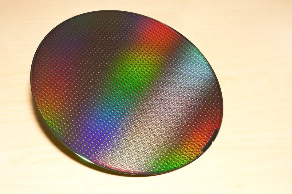
The fabrication of the ASIC involves several steps. First, the layout is transferred onto a silicon wafer using photolithography. This involves coating the wafer with a light-sensitive material, and then shining light through a mask that has the layout pattern on it. The light causes the material to harden in the areas where it hits, creating a physical representation of the layout on the wafer.
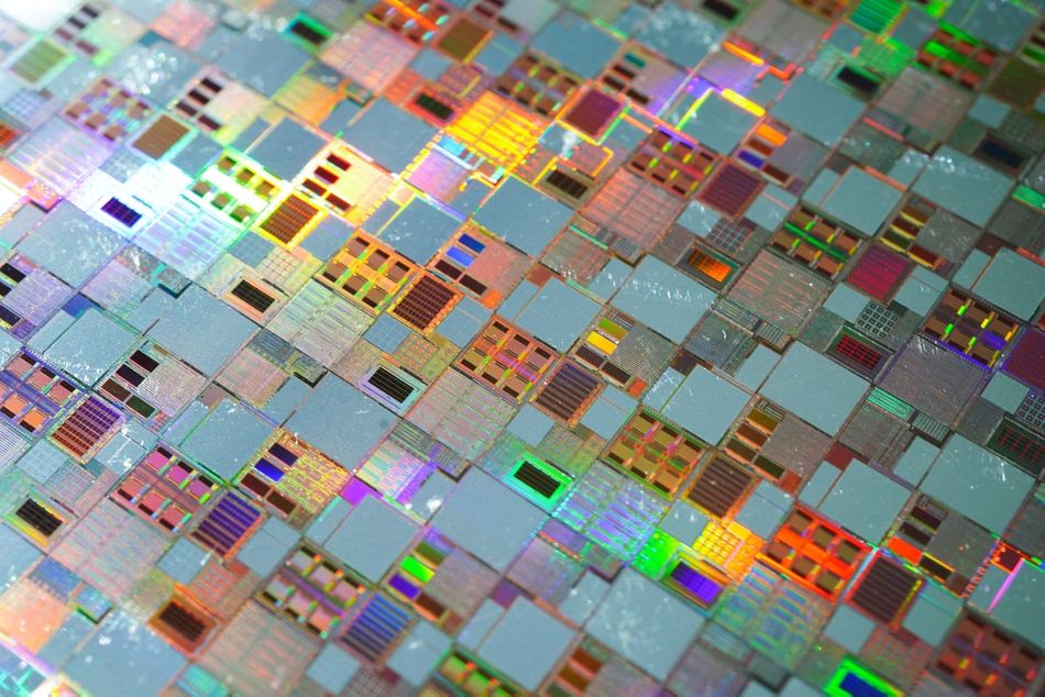
Next, the wafer is subjected to a series of chemical processes that etch away the unwanted material and deposit layers of different materials to form the transistors and interconnections. Once the fabrication process is complete, the wafer is cut into individual chips, each of which is an ASIC.
The design and fabrication of ASICs require a high level of expertise and sophisticated tools. However, the result is a chip that is highly efficient and powerful, capable of performing specific tasks with a level of performance that is difficult to achieve with general-purpose processors.
Programming ASICs
Programming an ASIC involves embedding a specific set of instructions directly into the circuit during the design phase. Unlike general-purpose processors that can be programmed with various software after manufacturing, ASICs are typically not reprogrammable. The programming of an ASIC is inherently linked to its design; therefore, the functionality of an ASIC is determined before it is fabricated.
The process begins with the development of a detailed specification that outlines the desired behavior of the ASIC. Engineers then translate these specifications into a hardware description language (HDL), such as Verilog or VHDL. HDLs are used to describe the structure and behavior of electronic circuits, and in the case of ASICs, they define how the ASIC will process data and execute tasks. [3]
Once the HDL code is written, it undergoes a simulation process to ensure the logic is correct and the ASIC will function as intended. This step is crucial as it is much more cost-effective to catch and correct errors in the simulation phase than after manufacturing the ASIC.
After successful simulation, the HDL code is synthesized into a physical layout, which includes the placement of transistors and the routing of electrical connections. This layout is then used to create photomasks, which are essential for the lithography process in semiconductor fabrication.
The final step in programming an ASIC is the actual fabrication, where layers of semiconductor material are built up on a silicon wafer, and the photomasks are used to pattern these layers, creating the physical ASIC. Once fabricated, the ASIC contains the programmed logic and is ready to be integrated into electronic devices.
It's important to note that some ASICs, known as Field-Programmable Gate Arrays (FPGAs), do allow for post-manufacturing programming. FPGAs contain an array of programmable logic blocks and interconnections that can be configured after fabrication. However, FPGAs are not as optimized for performance and power efficiency as ASICs that are programmed during the design phase.
Recommended Reading: Verilog vs VHDL: A Comprehensive Comparison
Types of ASICs
Application-Specific Integrated Circuits (ASICs) come in various types, each with its unique characteristics and uses. The different types of ASICs are primarily distinguished by the level of design customization involved in their creation. The three main types of ASICs are Full Custom, Semi-Custom, and Programmable ASICs.
Full Custom ASICs
Full Custom ASICs represent the highest level of customization in ASIC design. In a Full Custom ASIC, every aspect of the chip - from the individual transistors to the logic gates and the interconnections - is custom-designed to meet the specific requirements of the application. This allows for maximum optimization in terms of performance, power consumption, and chip area. [4]
Designing a Full Custom ASIC involves a significant amount of time and resources. It requires a deep understanding of semiconductor physics and electronic design, as well as access to sophisticated design tools. However, the result is a chip that is perfectly tailored to its application, offering the highest level of performance and efficiency.
Full Custom ASICs are typically used in applications where performance and efficiency are of utmost importance, and the high cost of design and fabrication can be justified. Examples of such applications include high-performance computing, advanced telecommunications systems, and high-end consumer electronics.
Despite their advantages, Full Custom ASICs have some drawbacks. The design flow is complex and time-consuming, and any changes or corrections require a complete chip redesign. Furthermore, the high cost of design and fabrication makes Full Custom ASICs unsuitable for low-volume applications. However, for applications that require the highest level of performance and efficiency, Full Custom ASICs are the ideal choice.
Semi-Custom ASICs
Semi-Custom ASICs offer a balance between customization and cost-effectiveness. Unlike Full Custom ASICs, where every aspect of the chip is custom-designed, Semi-Custom ASICs involve some pre-designed components. These pre-designed components, known as cells or blocks, are selected from a library and arranged to create the desired functionality.
There are two main types of Semi-Custom ASICs: Standard Cell-based ASICs and Gate Array-based ASICs. In Standard Cell-based ASICs, the design comprises a set of pre-designed logic cells that are arranged and interconnected to create the desired functionality. The cells are typically optimized for performance, power consumption, and area, allowing for a high level of customization while reducing chip design time and cost.
Gate Array-based ASICs, on the other hand, consist of a pre-fabricated chip with a large array of unconnected transistors. The final interconnections are added in the last few layers of the fabrication process, creating the desired functionality. This approach reduces fabrication time and cost, as the same base chip can be used for different designs. However, it offers less flexibility and performance compared to Standard Cell-based ASICs.
Semi-Custom ASICs are widely used in various applications, from consumer electronics to telecommunications systems. They offer a good balance between performance, power efficiency, and cost, making them a popular choice for many applications. However, they do not offer the same level of performance and efficiency as Full Custom ASICs, and they are not as flexible as Programmable ASICs.
Programmable ASICs
Programmable ASICs, also known as Field-Programmable Gate Arrays (FPGAs), are a unique class of ASICs which provide a flexible alternative to the fixed nature of traditional ASICs. Unlike Full Custom and Semi-Custom ASICs, which are designed with a fixed function in mind, FPGAs can be reprogrammed after manufacturing to perform different functions. This programmability is facilitated by an array of programmable logic blocks and a hierarchy of reconfigurable interconnects that allow the hardware to be adapted to different tasks post-fabrication.
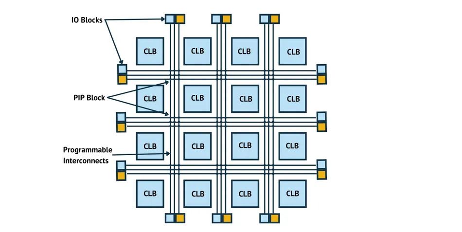
FPGAs comprise a matrix of configurable logic blocks (CLBs) connected via programmable interconnects. [5] Each CLB can perform various logical functions, and the interconnects can be programmed to create complex digital circuitry. The configuration of these blocks and interconnects is stored in a memory matrix within the FPGA, which can be written during the programming process. This process typically involves using a Hardware Description Language (HDL), such as RTL, Verilog or VHDL, similar to other types of ASICs.
The primary advantage of FPGAs is their flexibility. They can be used for prototyping and testing digital designs before committing to a fixed ASIC, significantly reducing development time and cost. Additionally, FPGAs are ideal for applications where the functionality may need to change over time, such as adaptive signal processing, software-defined radio, and various forms of digital communication systems.
However, this flexibility comes at a cost. FPGAs generally perform less than a dedicated ASIC due to the overhead of the programmable logic and interconnects. They also tend to consume more power and are more expensive on a per-unit basis. Despite these drawbacks, the ability to reconfigure the hardware for multiple applications without the need for a complete redesign makes FPGAs a valuable tool in the ASIC ecosystem.
Recommended Reading: FPGA Design: A Comprehensive Guide to Mastering Field-Programmable Gate Arrays
Applications of ASICs
Application-Specific Integrated Circuits (ASICs) are used in a wide range of applications due to their ability to perform specific tasks with high efficiency. Their customizability allows them to be tailored to the specific needs of an application, resulting in optimized performance, power consumption, and cost. ASICs are found in various industries, including telecommunications, automotive, consumer electronics, etc.
ASICs in Telecommunications
In the telecommunications industry, ASICs play a crucial role in enabling high-speed, reliable communication systems. They are used in various network parts, from the core network infrastructure to the end-user devices.
In network infrastructure, ASICs are used in routers and switches to handle the high-speed processing of data packets. They enable these logic devices to route data at high speeds with low latency, which is critical for maintaining the performance of the network. For instance, Cisco's Silicon One, a networking ASIC, can process up to 10.8 Terabits per second, enabling high-speed data transfer in modern networks. [6]
In end-user devices, such as cell phones and modems, ASICs handle various tasks, including signal processing, power management, and connectivity. For example, the baseband processor in a smartphone, which handles all communication functions, is typically an ASIC designed for this specific task. This allows the device to efficiently process signals, manage power, and maintain connectivity, enhancing the user experience.
The use of ASICs in telecommunications is expected to grow with the continued development of high-speed networks, such as 5G and beyond. These networks require high-performance, power-efficient devices to handle the increased data rates and low latency requirements, making ASICs an ideal solution.
ASICs in Cryptocurrency Mining
Cryptocurrency mining is another area where ASICs have found significant applications. Mining involves solving complex mathematical problems to validate transactions and add them to a blockchain. This process requires substantial computational power and energy, making the efficiency of ASICs highly beneficial.

ASICs used in cryptocurrency mining are designed to perform the specific hashing algorithms required by different cryptocurrencies. For instance, Bitcoin mining ASICs are optimized to perform the SHA-256 hashing algorithm, which is used in the Bitcoin proof-of-work system. These ASICs can perform the SHA-256 calculations much faster and more efficiently than general-purpose processors, making them ideal for Bitcoin mining.
One of the most well-known Bitcoin mining ASICs is the Antminer series from Bitmain. For example, the Antminer S19 Pro, one of the most powerful models, offers a hash rate of 110 Terahashes per second (TH/s) with a power efficiency of 29.5 Joules per Terahash (J/TH). [7] This high performance and efficiency make it a popular choice among Bitcoin miners.
However, using ASICs in cryptocurrency mining has also raised concerns about centralization. Because ASICs are expensive and specialized, they can be out of reach for individual miners, leading to a concentration of mining power in a few large mining farms. This centralization can potentially undermine the decentralized nature of cryptocurrencies.
Despite these concerns, the use of ASICs in cryptocurrency mining is likely to continue due to their superior performance and efficiency. As the complexity of mining algorithms increases and the reward for mining decreases, the efficiency provided by ASICs becomes increasingly important for profitable mining.
ASICs in Consumer Electronics
Consumer electronics is another significant area where ASICs are extensively used. These devices, including smartphones, tablets, smart TVs, and gaming consoles, require high-performance, power-efficient chips to deliver the features and user experience consumers demand.
In smartphones, for example, ASICs are used for various functions. The System on Chip (SoC), which is essentially an ASIC, integrates multiple components of a computer or other system into a single chip. This includes the CPU, GPU, memory, and more. For instance, Apple's A14 Bionic chip, used in the iPhone 12 series, is an SoC that includes a 6-core CPU, 4-core GPU, 16-core Neural Engine for AI tasks, and more, all in a single chip. [8]
In gaming consoles, ASICs are used to deliver high-performance graphics and audio. The PlayStation 5, for example, uses a custom ASIC for its GPU, capable of 10.28 teraflops of computing power and supports advanced features like ray tracing.
In smart TVs, ASICs handle video processing, including upscaling, motion smoothing, and color enhancement. For instance, Intel or Samsung's Quantum Processor 4K, used in their QLED TVs, is an ASIC that uses AI to upscale content to 4K resolution and optimize the picture quality scene by scene.
The use of ASICs in consumer electronics allows these devices to deliver high performance and rich features while maintaining power efficiency and compact form factors. As consumer demand for more advanced features and better user experience continue to grow, the role of ASICs in consumer electronics is expected to expand.
Recommended Reading: ASIC vs FPGA: A Comprehensive Comparison
Conclusion
ASICs play a crucial role in modern technology. They are specialized chips tailored for specific functions, offering optimal efficiency and performance. ASICs' evolution, from simple circuit designs to complex architectures, reflects the rapid advancement in semiconductor technology and electronic design methodologies. Full Custom ASICs provide peak performance for high-demand applications, while Semi-Custom ASICs balance customization and cost. Programmable ASICs, like FPGAs, offer unmatched flexibility and performance. ASICs largely impact industries like telecommunications, cryptocurrency mining, consumer electronics and IoT, driving innovation and efficiency. As technology advances, the importance of ASICs will continue to rise, meeting the growing demand for faster, more efficient, and smarter devices.
Frequently Asked Questions (FAQs)
Q. What is an ASIC, and why is it important?
A. An ASIC, or Application-Specific Integrated Circuit, is a chip designed for a specific application rather than for general-purpose use. Its importance lies in its ability to perform dedicated functions more efficiently than general-purpose processors, leading to better performance and power savings in electronic devices.
Q. How do ASICs differ from general-purpose processors?
A. ASICs are tailored for a specific function, analog or set of functions and are optimized for performance, power consumption, and size for that specific task. In contrast, general-purpose processors are designed to handle a wide range of tasks but may not be as efficient in any single task as an ASIC.
Q. What are the types of ASICs?
A. The main types of ASICs are Full Custom, Semi-Custom, and Programmable ASICs. Full Custom ASICs are entirely custom-designed, Semi-Custom ASICs use pre-designed electronic components, and Programmable ASICs, like FPGAs, can be reprogrammed after the manufacturing process.
Q. Where are ASICs used?
A. ASICs are used in various fields, including telecommunications, cryptocurrency mining, consumer electronics, automotive systems, and more. They are essential in devices that require intellectual property, high efficiency and performance for specific tasks.
Q. Can ASICs be reprogrammed?
A. Most ASICs are not reprogrammable once manufactured. However, a subset of ASICs known as FPGAs (Field-Programmable Gate Arrays) can be reprogrammed to perform different functions after fabrication.
Q. What are the challenges associated with ASICs?
A. Challenges include the high cost and complexity of design and manufacturing, particularly for Full Custom design ASICs. Additionally, the specialized nature of ASICs means they are not as flexible as general-purpose processors for different tasks.
References
[1] Computer History Museum. 1967: APPLICATION SPECIFIC INTEGRATED CIRCUITS EMPLOY COMPUTER-AIDED DESIGN [Cited 2024 February 28] Available at: Link
[2] Vinodsblog. Powerful AI Chips: Powering the Future of Intelligence [Cited 2024 February 28]
[3] Wevolver. Verilog vs VHDL: A Comprehensive Comparison [Cited 2024 February 28] Available at: Link
[4] Wevolver. The Ultimate Guide to ASIC Design: From Concept to Production [Cited 2024 February 28] Available at: Link
[5] D-Central. Inside the ASIC Fabrication Process: From Concept to Completion [Cited 2024 February 28] Available at: Link
[6] Cisco. Cisco Silicon One Q100 and Q100L Processors Data Sheet [Cited 2024 February 28] Available at: Link
[7] TechBullion. The Top Bitcoin Mining Hardware: Maximizing Profits in the Crypto Space [Cited 2024 February 28] Available at: Link
[8] Macworld. A14 Bionic FAQ: What you need to know about Apple’s 5nm processor [Cited 2024 February 28] Available at: Link