PWB vs PCB: Differences and Similarities
PWB and PCB are two commonly inter-used terms in the industry of consumer electronics. The former means printed wiring board and the latter, short for printed circuit board. This article explores their similarities and subtle differences; their uses, types, and benefits to the electronics industry.

12 Sep, 2023. 21 minutes read
Hight tech electronic PCB
Introduction
Printed Wiring Boards (PWB) and Printed Circuit Boards (PCB) are essential components in modern electronics, serving as the foundation for connecting and supporting various electronic products and components. The terms PWB and PCB are often used interchangeably, but they have a few differences in their design, manufacturing process, and applications.
This article will delve into the definitions, components, and manufacturing processes of both PWBs and PCBs, as well as explore their key differences, applications, and factors to consider when choosing between the two. By gaining a deeper understanding of PWBs and PCBs, readers will be better equipped to make informed decisions in their electronic design and manufacturing endeavors.
Printed Wiring Boards (PWB)
Definition and Overview
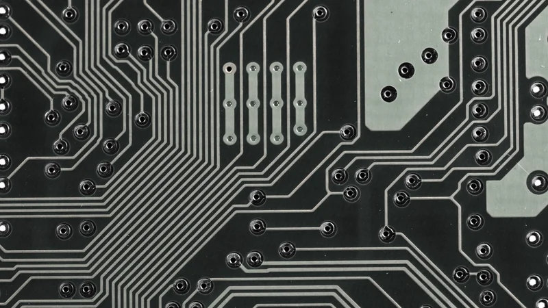
Printed Wiring Boards (abbreviation: PWB) are the precursors to Printed Circuit Boards (abbreviation: PCB) and serve as the foundation for connecting electronic components. PWBs consist of conductive pathways, or traces, that are printed or etched onto a non-conductive substrate. These traces form the electrical connections between components, enabling the flow of current and communication between devices.
In the early stages of electronics, PWBs were primarily used for simple connections and did not include any embedded components. The main function of a PWB is to provide a physical platform for mounting and interconnecting electronic components, such as resistors, capacitors, and integrated circuits (ICs). PWBs are typically single-sided, meaning that the conductive traces are only present on one side of the substrate. This design limitation restricts the complexity of circuits that can be implemented on a PWB, making them more suitable for simpler electronic devices and applications.
The design substrate material used in PWBs is crucial for its performance and durability. Commonly used materials include phenolic paper, epoxy glass, and polyimide. Phenolic paper is an inexpensive option, offering moderate electrical insulation and mechanical strength. Epoxy glass provides better electrical insulation and mechanical stability, making it suitable for more demanding applications. Polyimide is a high-performance material with excellent thermal stability and chemical resistance, ideal for use in aerospace and military applications where extreme conditions are encountered.
Components and Materials
The main components of a PWB include the substrate, conductive traces, and through-holes or vias. The substrate is the non-conductive material that provides mechanical support and electrical insulation for the conductive traces. As mentioned earlier, common substrate materials for PWBs are phenolic paper, epoxy fiberglass, prepreg, and polyimide, each offering different levels of performance and cost.
Conductive traces are the thin lines of conductive material, typically copper, that form the electrical connections between components on the PWB. Copper is the most widely used material for traces due to its excellent electrical conductivity, low cost, and ease of processing. The thickness of the copper traces can vary depending on the current-carrying capacity requirements and electronics manufacturing constraints. Thicker traces can handle higher currents but may require more complex manufacturing processes.
Through-holes or vias are used to connect traces on different layers of the PWB or to provide mounting points for electronic components. In single-sided PWBs, through-holes are primarily used for component mounting, while in double-sided or multilayer PWBs, they can also serve as interconnections between layers. Plated through-holes (PTH) are created by depositing a thin layer of conductive material, such as copper, on the walls of the hole, providing an electrical connection between layers.
Further reading: What is a Via: A Comprehensive Guide
In addition to the core components, PWBs may also incorporate various surface finishes to protect the exposed copper traces from oxidation and improve solderability. Common surface finishes include Hot Air Solder Leveling (HASL), Electroless Nickel Immersion Gold (ENIG), and Organic Solderability Preservative (OSP). Each finish offers different levels of protection, solderability, and cost, making them suitable for different applications and manufacturing requirements.
Manufacturing Process
The first step in the PCB manufacturing process is to get the PCB design ready. Engineers and designers use specialized software to layout the circuitry, position components, and define the connections between them. Once the design is finalized, it's translated into a format known as a 'Gerber file.' This file serves as the blueprint for the manufacturing process, detailing every aspect of the board's layout, from conductor paths to component placements. Only with a meticulously crafted design can the manufacturing process commence, ensuring that the final product aligns perfectly with the intended electronic functionality and performance specifications. At any point of the manufacturing process, if issues are detected during inspection, the board may undergo a rework process to correct any anomalies.
Japan holds a significant position in the innovation and development of sophisticated PCB technologies, often pioneering advancements in design substrate materials and manufacturing processes that cater to the high precision requirements.
The hardware manufacturing process of PWBs involves several key steps, including substrate preparation, pattern generation, etching, and surface finishing. Each step plays a crucial role in determining the final quality and performance of the PWB.
- Substrate preparation: The first step in PWB manufacturing is preparing the substrate material. This involves cutting the substrate to the desired size and cleaning its surface to remove any contaminants that could interfere with the adhesion of the conductive traces. Depending on the substrate material, additional treatments may be required to enhance its surface properties, such as roughening the surface to improve adhesion or applying a thin layer of conductive material for electroless plating processes.
- Pattern generation: The next step is to create the desired circuit pattern on the substrate. This can be achieved through various methods, such as photolithography, screen printing, or direct imaging. Photolithography involves applying a photosensitive resist material to the substrate, exposing it to ultraviolet light through a photomask with the desired pattern, and then developing the resist to reveal the pattern. Screen printing uses a stencil or screen to apply the resist material in the desired pattern directly onto the substrate. Direct imaging techniques, such as laser direct imaging (LDI), use a computer-controlled laser to expose the resist material without the need for a photomask.
- Etching: Once the pattern has been generated, the exposed areas of the substrate are etched away, leaving behind the conductive traces. This is typically done using chemical etchants, such as ferric chloride or ammonium persulfate, which selectively dissolve the exposed conductive material. The remaining resist material is then removed, revealing the final circuit pattern.

- Surface finishing: The final step in PWB manufacturing is to apply a surface finish to the exposed copper traces. This protects the copper from oxidation and improves solderability during component assembly. As mentioned earlier, common surface finishes include Hot Air Solder Leveling (HASL), Electroless Nickel Immersion Gold (ENIG), and Organic Solderability Preservative (OSP). The choice of surface finish depends on factors such as cost, performance requirements, and compatibility with the intended assembly process.
After the surface finishing, the PWB may undergo additional processes, such as drilling holes for component mounting and through-hole connections, as well as quality control inspections to ensure the board meets the required specifications.
Over the last two decades, China emerged as a powerhouse in the electronics manufacturing sector, often being the go-to destination for mass production of both PWBs and PCBs, leveraging advanced PCB fabrication techniques to meet the growing demands of various industries. In the post-covid era, cloud manufacturing has gained prominence, offering a decentralized approach to production, enhancing supply chain resilience.
Further reading: Cloud Manufacturing Services Deliver New PCB Possibilities
Printed Circuit Boards (PCB)
Definition and Overview
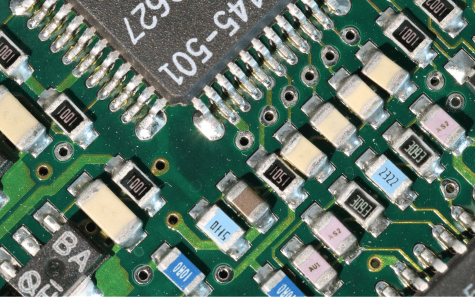
Printed Circuit Boards (PCB) are the more advanced successors to Printed Wiring Boards (PWB), providing a platform for mounting and interconnecting electronic components in complex circuits. PCBs consist of multiple layers of conductive traces and insulating materials, allowing for greater design flexibility and higher component density compared to PWBs. The traces on a PCB are typically made of copper, which is known for its excellent electrical conductivity and compatibility with various manufacturing processes.
PCBs can be single-sided, double-sided, or multilayer, depending on the complexity of the circuit and the desired performance characteristics. Single-sided PCBs have conductive traces on one side of the substrate, while double-sided PCBs have traces on both sides. Multilayer PCBs consist of multiple layers of conductive traces and insulating materials, allowing for more complex circuit designs and improved signal integrity.
The term PCB refers to a board that provides a stable and reliable platform for mounting and interconnecting electronic components, such as resistors, capacitors, diodes, transistors, ICs, and connectors. PCBs are used in a wide range of applications, from simple consumer electronics to advanced aerospace and military systems, due to their versatility, performance, and reliability.
Components and Materials
The main components of a PCB include the substrate, conductive traces, vias, and solder mask. Each of these components plays a critical role in the performance and reliability of the PCB.
- Substrate: The substrate is the base material that provides mechanical support and electrical insulation for the conductive traces. Common substrate materials for PCBs include FR-4, a glass-reinforced epoxy laminate, and high-performance materials such as polyimide and Rogers materials. FR-4 is the most widely used substrate material due to its good electrical insulation, mechanical strength, and cost-effectiveness. High-performance materials offer improved thermal stability, lower dielectric loss, and better dimensional stability, making them suitable for demanding applications such as high-frequency circuits and high-temperature environments.
- Conductive traces: Copper is the most common material used for conductive traces on PCBs due to its excellent electrical conductivity, low cost, and compatibility with various manufacturing processes. The thickness of the copper traces can vary depending on the current-carrying capacity requirements and manufacturing constraints. Thicker traces can handle higher currents but may require more complex manufacturing processes, such as electroplating or laminating multiple layers of copper foil.
- Vias: Vias are small holes in the PCB that provide electrical connections between different layers of conductive traces or serve as mounting points for electronic components. There are several types of vias, including through-hole vias, blind vias, and buried vias. Through-hole vias connect the top and bottom layers of the PCB, while blind vias connect an outer layer to one or more inner layers without penetrating the entire board. Buried vias connect two or more inner layers without being exposed on the outer layers.
- Solder mask: The solder mask is a thin layer of insulating material, usually a polymer, that is applied to the surface of the PCB to protect the conductive traces from oxidation, contamination, and short-circuits during component assembly. The solder mask also helps to improve the solderability of the PCB by preventing solder bridges between adjacent traces. Common solder mask materials include liquid photoimageable (LPI) solder mask, dry film solder mask, and screen-printed solder mask. Each type of solder mask offers different levels of resolution, thickness, and cost, making them suitable for different applications and manufacturing requirements.
Further reading: Components of a PCB: A Comprehensive Guide
Manufacturing Process
The manufacturing process of PCBs involves several key steps, including substrate preparation, pattern generation, etching, drilling, plating, and surface finishing. Each step plays a crucial role in determining the final quality and performance of the PCB.
Further reading: PCB Material: A Comprehensive Guide to Understanding and Choosing the Right Materials
Substrate preparation: The first step in PCB manufacturing is preparing the substrate material. This involves cutting the substrate to the desired size, cleaning its surface to remove any contaminants, and applying a thin layer of copper foil on one or both sides of the substrate. The copper foil serves as the base material for the conductive traces and is typically laminated onto the substrate using heat and pressure.
Pattern generation: The next step is to create the desired circuit pattern on the copper foil. This can be achieved through various methods, such as photolithography, laser direct imaging (LDI), or inkjet printing. Photolithography involves applying a photosensitive resist material to the copper foil, exposing it to ultraviolet light through a photomask with the desired pattern, and then developing the resist to reveal the pattern. LDI uses a computer-controlled laser to expose the resist material without the need for a photomask. Inkjet printing directly deposits etch-resistant ink onto the copper foil in the desired pattern.
Etching: Once the pattern has been generated, the exposed areas of the copper foil are etched away, leaving behind the conductive traces. This is typically done using chemical etchants, such as ferric chloride or ammonium persulfate, which selectively dissolve the exposed copper. The remaining resist material is then removed, revealing the final circuit pattern.
Drilling: After etching, holes are drilled into the PCB for component mounting and through-hole connections. The size and location of the holes are determined by the PCB design and component requirements. Drilling is typically performed using computer numerical control (CNC) machines, which provide high precision and repeatability.
Plating: To create electrical connections between layers and improve the solderability of the drilled holes, a thin layer of conductive material, such as copper, is deposited onto the walls of the holes. This process, known as plating, can be achieved through electroless plating or electroplating. Electroless plating involves immersing the PCB in a chemical solution that deposits a thin layer of copper onto the hole walls without the need for an external electrical current. Electroplating uses an external electrical current to deposit the copper onto the hole walls.
Surface finishing: The final step in PCB manufacturing is to apply a surface finish to the exposed copper traces. This protects the copper from oxidation and improves solderability during component assembly. Common surface finishes include Hot Air Solder Leveling (HASL), Electroless Nickel Immersion Gold (ENIG), and Organic Solderability Preservative (OSP). The choice of surface finish depends on factors such as cost, performance requirements, and compatibility with the intended assembly process.
Further reading: PCB Manufacturing Process: Everything You Need to Know
After the surface finishing, the PCB undergoes additional processes, such as solder mask application, silkscreen printing, and quality control inspections, to ensure the board meets the required specifications and is ready for component assembly.
Key Differences between PWB and PCB
Terminology and Usage
One of the primary differences between PWB and PCB lies in the terminology and usage of the terms. While both PWB and PCB refer to the foundation for connecting and supporting electronic components, the term PWB is often associated with simpler, single-sided boards with only conductive traces and no embedded components. On the other hand, PCB is a more encompassing term that includes single-sided, double-sided, and multilayer boards with varying levels of complexity and component integration.
The distinction between PWB and PCB can be traced back to the historical development of these technologies. In the early days of electronics, PWBs were the primary means of interconnecting components, and the term "printed wiring board" accurately described their function as a platform for wiring electronic components together. As technology advanced and electronic devices became more complex, the need for more sophisticated interconnections led to the development of PCBs, which incorporated multiple layers of conductive traces and embedded components.
Despite the differences in terminology, it is important to note that the terms PWB and PCB are often used interchangeably in the electronics industry. This can sometimes lead to confusion, especially when discussing specific board types or manufacturing processes. To avoid misunderstandings, it is essential to clarify the intended meaning of the terms when discussing the design, manufacturing, or application of printed boards in electronic devices.
Design Complexity
Another key difference between PWBs and PCBs is the level of design complexity they can accommodate. PWBs are typically single-sided, with conductive traces only on one side of the substrate. This design limitation restricts the complexity of circuits that can be implemented on a PWB, making them more suitable for simpler electronic devices and applications. In contrast, PCBs can be single-sided, double-sided, or multilayer, allowing for greater design flexibility and higher component density.
Double-sided PCBs have conductive traces on both sides of the substrate, enabling more complex circuit designs and increased component density compared to single-sided PWBs. The use of through-holes or vias allows for electrical connections between the top and bottom layers, further enhancing the design capabilities of double-sided PCBs.
Multilayer PCBs take design complexity to an even higher level by incorporating multiple conductive layers of conductive traces and insulating materials. This allows for more intricate circuit designs, improved signal integrity, and better thermal management. Multilayer PCBs can have anywhere from four to over 30 layers, depending on the application requirements and manufacturing constraints. The increased design complexity of multilayer PCBs enables them to support advanced electronic devices and systems, such as high-speed digital circuits, high-frequency RF circuits, and high-density interconnects (HDI).
In summary, the design complexity of PWBs and PCBs varies significantly, with PWBs being more suitable for simpler applications and PCBs offering greater flexibility and performance for more advanced electronic devices. Understanding the board design capabilities of each board type is essential when selecting the appropriate technology for a specific project or application.
Manufacturing Techniques
The manufacturing techniques used for PWB assemblies and PCB assemblies also differ slightly, reflecting the varying levels of design complexity and performance requirements associated with each board type. PWB manufacturing typically involves simpler processes, such as photolithography or screen printing for pattern generation and chemical etching for trace formation. These techniques are well-suited for single-sided boards with relatively simple circuit designs and lower component densities.
PCB manufacturing, on the other hand, requires more advanced techniques to accommodate the increased design complexity and performance demands of modern electronic devices. For example, laser direct imaging (LDI) or inkjet printing may be used for pattern generation, offering higher resolution and accuracy compared to photolithography or screen printing. Additionally, PCB manufacturing often involves more complex drilling and plating processes to create through-holes, blind vias, and buried vias for interconnecting multiple layers of conductive traces.
Multilayer PCB manufacturing adds further complexity to the process, requiring precise alignment and lamination of multiple layers of conductive traces and insulating materials. This involves the use of specialized equipment, such as vacuum presses and optical alignment systems, to ensure accurate registration and bonding of the layers. The manufacturing process for multilayer PCBs also includes additional steps, such as sequential build-up (SBU) or semi-additive processes (SAP), to create fine-pitch interconnects and high-density circuits.
In summary, the manufacturing techniques for PWBs and PCBs differ significantly, with PWB manufacturing involving simpler processes and PCB manufacturing requiring more advanced techniques to accommodate the higher design complexity and performance requirements of modern electronic devices. Understanding the manufacturing capabilities and constraints associated with each board type is essential when selecting the appropriate technology for a specific project or application.
To sum up the discussion, here is a table comparing PWBs and PCBs based on various criteria:
Criteria | PWB | PCB |
Design Complexity | Typically single-sided. Suitable for simpler electronic devices and applications. | Can be single-sided, double-sided, or multilayer. Greater design flexibility and higher component density. |
Manufacturing Techniques | Simpler processes like photolithography or screen printing. | Advanced techniques like laser direct imaging or multilayer lamination. |
Material Selection | Typically phenolic paper or epoxy glass. Though other options are also viable. | Typically FR-4, polyimide, Rogers materials. Though other options are also viable. |
Performance and Reliability | Basic electronic functionality. | Better signal integrity, thermal management, and mechanical stability. |
Industry Standards | Might adhere to simpler industry standards. | Often adheres to stringent standards set by bodies like IPC. |
Terminology Use | Less frequent in industry. | Frequently used in the industry. |
Post-Design Process | Involves basic electronics manufacturing. | Involves advanced electronics manufacturing, reflow, and potential rework. |
Board Type | Often referred to as a "bare board". | Might be part of a printed circuit board assembly (PCBA) or printed wiring assembly (PWA). |
Applications | Consumer electronics, power supplies, industrial controls, some automotive electronics. | Computers, smartphones, telecommunications equipment, medical devices, aerospace systems, advanced automotive electronics. |
Applications of PWBs and PCBs
PWB Applications
Due to their simpler design and lower manufacturing complexity, PWBs are well-suited for applications that require basic electronic functionality and do not demand high component density or advanced circuit designs. Some common applications of PWBs include:
Consumer electronics: PWBs can be found in various consumer electronic devices, such as remote controls, calculators, and simple toys. These devices typically have lower component density and simpler circuit designs, making PWBs a cost-effective and suitable choice for their electronic interconnections.
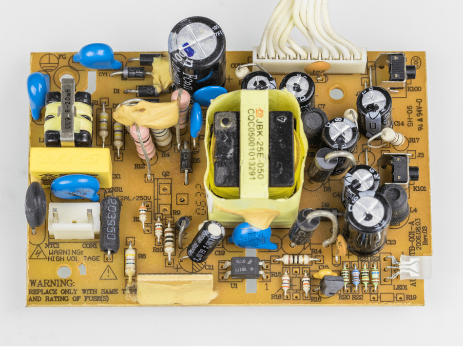
Power supplies: PWBs are often used in power supply units, such as AC/DC converters and battery chargers, where the primary function is to distribute power to other electronic components. In these applications, the focus is on providing reliable power connections rather than complex signal routing or high-speed data transmission.
Industrial controls: PWBs can be used in industrial control systems, such as motor controllers, temperature sensors, and relay boards, where the primary function is to monitor and control various processes and equipment. In these applications, the electronic circuits are typically less complex, and the emphasis is on robustness and reliability rather than high-speed performance or miniaturization.
Automotive electronics: PWBs can be found in some automotive electronic systems, such as lighting controls, simple dashboard displays, and basic sensor interfaces. These applications often require durable and reliable electronic connections but do not demand the high component density or advanced circuit designs found in more sophisticated automotive systems, such as engine control units or advanced driver assistance systems (ADAS).
In summary, PWBs are well-suited for applications that require basic electronic functionality, lower component density, and simpler circuit designs. Their lower manufacturing complexity and cost make them an attractive choice for a wide range of electronic devices and systems.
PCB Applications
PCBs, with their increased design complexity and advanced manufacturing techniques, are suitable for a wide range of applications that demand higher component density, intricate circuit designs, and improved performance. Modern PCBs utilize technologies like surface mount technology (SMT) to attach components, allowing for more compact and efficient designs. Some common applications of PCBs include:
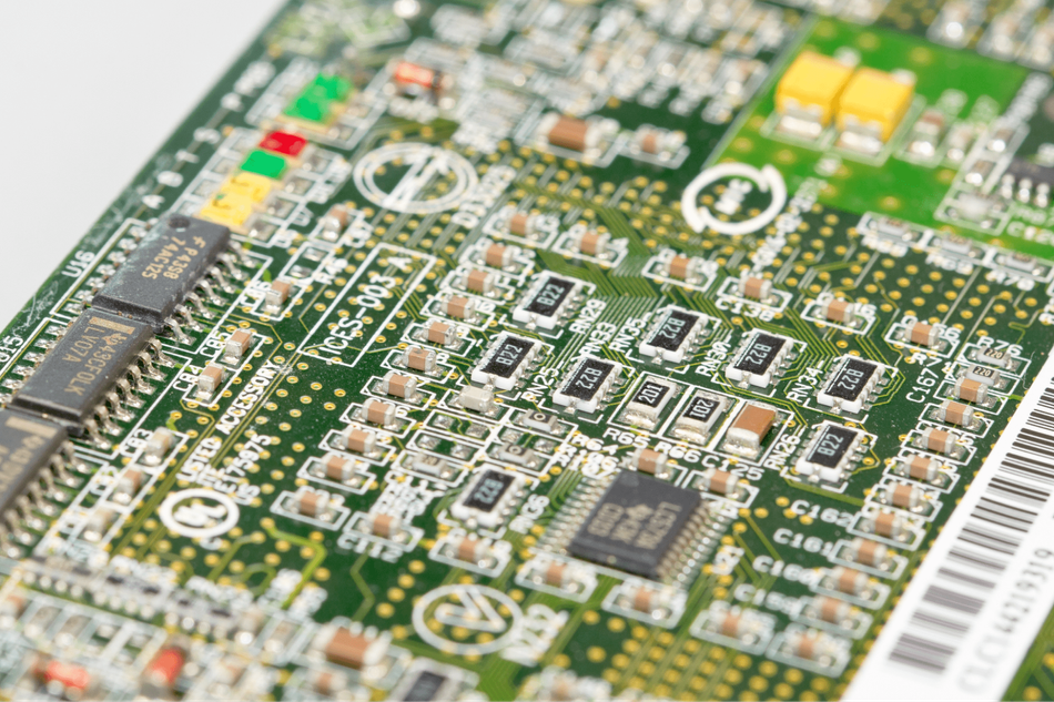
Computers and smartphones: PCBs are essential components in modern computers, smartphones, and tablets, where they provide the foundation for mounting and interconnecting high-density components, such as processors, memory chips, and communication modules. The advanced circuit designs and multilayer construction of PCBs enable high-speed data transmission and efficient power distribution, which are critical for the performance of these devices.
Telecommunications equipment: PCBs are widely used in telecommunications equipment, such as routers, switches, and base stations, where they support high-frequency signal transmission and complex digital signal processing. The use of high-performance substrate materials and advanced manufacturing techniques, such as controlled impedance and blind/buried vias, ensures signal integrity and minimizes signal loss in these applications.
Medical devices: PCBs are found in various medical devices, such as diagnostic imaging systems, patient monitoring devices, and implantable electronics, where they provide reliable and precise electronic interconnections. The stringent performance and reliability requirements of medical devices often necessitate the use of high-quality materials and manufacturing processes, such as high-temperature laminates and gold plating for improved corrosion resistance.
Aerospace and defense systems: PCBs are used in aerospace and defense systems, such as avionics, radar systems, and satellite communications, where they must withstand extreme environmental conditions and meet strict performance specifications. In these applications, PCBs often incorporate high-performance materials, such as polyimide or Rogers materials, and advanced manufacturing techniques, such as sequential build-up (SBU) or high-density interconnects (HDI), to ensure optimal performance and reliability.
Automotive electronics: Advanced automotive electronic systems, such as engine control units, advanced driver assistance systems (ADAS), and infotainment systems, rely on PCBs for their electronic interconnections. These applications require PCBs with high component density, robust thermal management, and reliable performance under harsh operating conditions, such as temperature extremes and vibration.
In summary, PCBs are suitable for a wide range of applications that demand higher component density, complex circuit designs, and improved performance. Their versatility and advanced manufacturing capabilities make them an essential component in modern electronic devices and systems.
Choosing Between PWB and PCB
Factors to Consider
When selecting between PWB and PCB for a specific project or application, several factors must be considered to ensure the appropriate technology is chosen. These factors include:
- Design complexity: The complexity of the circuit design is a critical factor in determining whether a PWB or PCB is more suitable. PWBs are well-suited for simpler designs with lower component density, while PCBs offer greater design flexibility and can accommodate more complex circuits with higher component density.
- Performance requirements: The performance requirements of the electronic device or system play a significant role in the choice between PWB and PCB. PCBs generally offer better signal integrity, thermal management, and reliability compared to PWBs, making them more suitable for applications that demand high-speed data transmission, efficient power distribution, or operation under harsh environmental conditions.
- Manufacturing constraints: The manufacturing capabilities and constraints of the chosen technology must be considered when selecting between PWB and PCB. PWB manufacturing typically involves simpler processes and lower costs, making it an attractive option for low-volume production or applications with tight budget constraints. PCB manufacturing, on the other hand, requires more advanced techniques and equipment, which can result in higher costs and longer lead times. However, the increased design flexibility and performance offered by PCBs may justify the additional investment in certain applications.
- Material selection: The choice of substrate material can impact the performance, durability, and cost of the final product. PWBs typically use lower-cost materials, such as phenolic paper or epoxy glass, which may be sufficient for less demanding applications. PCBs often employ higher-performance materials, such as FR-4, polyimide, or Rogers materials, to meet the more stringent performance and reliability requirements of advanced electronic devices and systems.
- Regulatory and industry standards: Depending on the application, specific regulatory or industry standards may dictate the choice between PWB and PCB. For example, certain medical, aerospace, or automotive applications may require the use of PCBs with specific material properties, manufacturing processes, or performance characteristics to meet regulatory requirements or industry standards.
By carefully considering these factors, engineers, designers, and manufacturers can make informed decisions when selecting between PWB and PCB for their electronic design and manufacturing projects.
Cost and Budget Considerations
Cost and budget constraints play a significant role in the decision-making process when choosing between PWB and PCB. Several factors contribute to the overall cost of each board type, including material selection, manufacturing processes, and design complexity.
- Material costs: PWBs typically use lower-cost materials, such as phenolic paper or epoxy glass, which can result in lower overall costs compared to PCBs. PCBs often employ higher-performance materials, such as FR-4, polyimide, or Rogers materials, which can increase the cost of the substrate. Additionally, the choice of surface finishes, such as HASL, ENIG, or OSP, can also impact the overall cost of the board.
- Manufacturing costs: PWB manufacturing generally involves simpler processes and lower costs compared to PCB manufacturing. The simpler design and single-sided nature of PWBs allow for more straightforward manufacturing techniques, such as photolithography or screen printing for pattern generation and chemical etching for trace formation. In contrast, PCB manufacturing requires more advanced techniques, such as LDI, inkjet printing, or multilayer lamination, which can result in higher costs and longer lead times.
- Design complexity: The complexity of the circuit design can also impact the cost of the board. PWBs are well-suited for simpler designs with lower component density, which can result in lower overall costs. PCBs, with their increased design flexibility and higher component density, can accommodate more complex circuits but may require additional investment in design and manufacturing resources.
- Volume and economies of scale: The production volume can significantly influence the cost of both PWBs and PCBs. In low-volume production, the simpler manufacturing processes and lower material costs of PWBs may offer a cost advantage. However, as production volumes increase, the economies of scale can reduce the cost difference between PWBs and PCBs, making the latter a more viable option for high-volume production.
When considering cost and budget constraints, it is essential to weigh the trade-offs between the lower costs of PWBs and the increased design flexibility and performance offered by PCBs. By carefully evaluating these factors, engineers, designers, and manufacturers can make informed decisions that balance cost and performance requirements for their specific applications.
Performance and Reliability
When choosing between PWB and PCB, the performance and reliability requirements of the electronic device or system must be considered. These factors can significantly impact the suitability of each board type for a specific application.
- Signal integrity: PCBs generally offer better signal integrity compared to PWBs, due to their multilayer construction and advanced manufacturing techniques. The use of controlled impedance, blind/buried vias, and high-performance substrate materials can minimize signal loss and crosstalk, ensuring reliable high-speed data transmission and efficient power distribution. In applications where signal integrity is critical, such as high-speed digital circuits or high-frequency RF circuits, PCBs are the preferred choice.
- Thermal management: PCBs typically provide better thermal management than PWBs, due to their multilayer construction and the use of thermally conductive materials, such as metal-core substrates or embedded heat sinks. Effective thermal management is crucial for maintaining the performance and reliability of electronic devices, especially in high-power or high-temperature applications. In such cases, PCBs are more suitable than PWBs.
- Mechanical stability: The mechanical stability of the board is another important factor to consider when choosing between PWB and PCB. PCBs, with their multilayer construction and higher-quality substrate materials, generally offer better mechanical stability and resistance to warping, vibration, and thermal expansion compared to PWBs. This makes PCBs more suitable for applications where mechanical stability is critical, such as aerospace, automotive, or industrial systems.
- Environmental resistance: PCBs often incorporate higher-performance materials and surface finishes that provide better resistance to environmental factors, such as moisture, temperature extremes, and chemical exposure. This can result in improved reliability and longer service life for electronic devices and systems that operate in harsh environments or are subject to stringent regulatory requirements.
In summary, the performance and reliability requirements of the electronic device or system play a significant role in the choice between PWB and PCB. By carefully evaluating these factors, engineers, designers, and manufacturers can make informed decisions that balance cost and performance requirements for their specific applications. The final product might incorporate a custom-designed PWB combined with integrated third-party printed circuit assemblies (PCAs)/circuit cards.
Further reading: PCBA vs PCB: The foundation of modern-day electronics
Conclusion
In conclusion, understanding the differences between PWBs and PCBs is crucial for engineers, designers, and manufacturers when selecting the appropriate board type for a specific project or application. PWBs are well-suited for simpler designs with lower component density, while PCBs offer greater design flexibility and can accommodate more complex circuits with higher component density. The choice between PWB and PCB depends on factors such as design complexity, performance requirements, manufacturing constraints, material selection, and cost and budget considerations. By carefully evaluating these factors, informed decisions can be made that balance cost and performance requirements for specific applications.
Further reading: MacroFab - Wevolver
Frequently Asked Questions (FAQs)
1. What is the main difference between PWB and PCB?
The main difference between PWB and PCB lies in their design complexity and manufacturing techniques. PWBs are typically single-sided boards with simpler circuit designs, while PCBs can be single-sided, double-sided, or multilayer boards with more complex circuit designs and higher component density.
2. Can PWB and PCB be used interchangeably?
While the terms PWB and PCB are often used interchangeably in the electronics industry, they refer to different board types with varying levels of design complexity and performance. It is essential to clarify the intended meaning of the terms when discussing the design, manufacturing, or application of printed boards in electronic devices.
3. When should I choose a PWB over a PCB?
PWBs are more suitable for applications that require basic electronic functionality, lower component density, and simpler circuit designs. Their lower manufacturing complexity and cost make them an attractive choice for low-volume production or applications with tight budget constraints.
4. When should I choose a PCB over a PWB?
PCBs are more suitable for applications that demand higher component density, complex circuit designs, and improved performance. Their versatility and advanced manufacturing capabilities make them an essential component in modern electronic devices and systems.
5. How do the manufacturing processes of PWBs and PCBs differ?
PWB manufacturing typically involves simpler processes, such as photolithography or screen printing for pattern generation and chemical etching for trace formation. In contrast, PCB manufacturing requires more advanced techniques, such as laser direct imaging (LDI), inkjet printing, or multilayer lamination, to accommodate the increased design complexity and performance demands of modern electronic devices.
References
[1] Macrofab. The Ultimate PCBA Development Guide. [Internet]. 2023 Jan 19. Available from:
[2] Coombs, Clyde F., Jr., and Happy T. Holden, eds. 2016. Printed Circuits Handbook. 7th ed. New York: McGraw-Hill Education.
[3] Ott HW. Electromagnetic Compatibility Engineering. 1st ed. Wiley; 2009. Available from: https://doi.org/10.1002/9780470508510.ch1. ISBN: 9780470189306
in this article
1. Introduction2. Printed Wiring Boards (PWB)3. Components and Materials4. Manufacturing Process5. Printed Circuit Boards (PCB)6. Key Differences between PWB and PCB7. Applications of PWBs and PCBs8. PCB Applications9. Choosing Between PWB and PCB10. Conclusion11. Frequently Asked Questions (FAQs)12. References