PCB Manufacturing Process: A Comprehensive Guide to Understanding and Mastering the Techniques
Printed Circuit Boards (PCBs) provide the foundation for the assembly of electronic components and enable the functionality of a wide range of devices. This article journeys through the requisite steps in the PCB manufacturing process, detailing the procedures involved in each.

Last updated on 02 Feb, 2024. 23 minutes read
Assembly of Circuit Boards
Introduction
Printed circuit boards (PCBs) serve as electronic devices' mechanical and electrical backbone, connecting components through conductive pathways and signal traces on copper sheets laminated onto a non-conductive substrate. From household appliances to high-tech machines, PCBs are indispensable for the proper functioning of various electronic devices.
The PCB or circuit board manufacturing process is a sophisticated sequence of steps crucial to developing these essential components. Each critical stage demands meticulous attention to detail to ensure the flawless production of PCB prototypes or batches of PCB assemblies. Initiated with design and review stages employing PCB circuit board design CAD tools, the process is guided by computer and machine precision to prevent issues like short circuits or incomplete circuits.
The manufacturing journey encompasses a range of elements, including drill holes, epoxy resin, silkscreen, solder mask, inner layers, outer layers, surface finish, laminate, and photoresist. The boards undergo strict testing, including optical inspection and functional checks, at various fabrication points, culminating in a final assessment of complete boards before packaging and shipment.
Understanding the PCB or circuit board manufacturing process is paramount for electronics industry professionals. It provides valuable insights into the design, fabrication, and assembly of these critical components. This complex sequence involves techniques such as material selection, imaging, etching, drilling, and plating. The final assembly involves placing and soldering electronic components onto the fabricated board.
Quality control and reliability testing are integral aspects of the PCB manufacturing process, ensuring that the final product meets required standards and performs reliably under diverse conditions. In an era of increasing environmental awareness, sustainable manufacturing practices and waste management have become crucial considerations in the PCB industry.
What are PCBs?
A Printed Circuit Board (PCB) is a slim board manufactured from materials such as fiberglass, composite epoxy, or other laminate substances. Conductive pathways, often crafted from copper foil, are either etched or "printed" onto the board, forming connections among components like transistors, resistors, and integrated circuits.
Essentially, PCBs represent the tangible embodiment of electronic circuits, serving as the framework to both secure and establish electrical connections among electronic components. The term 'printed' in their name originates from the manufacturing process, where copper tracks are imprinted onto the board using tools like Gerber files, providing essential electrical pathways.
The PCB manufacturing process often involves using pre-impregnated ( also known as prepreg) material, contributing to the overall structural integrity and insulating properties of the board. Prepeg, combined with other elements like epoxy resin, plays a crucial role in the lamination process that results in a cohesive and durable PCB.
PCBs are omnipresent in modern electronics, spanning from uncomplicated devices like digital watches and calculators to intricate systems such as computers and satellites. Grasping the structure and functionality of PCBs is paramount to comprehending the operation of these diverse electronic devices.
Types of PCBs
Printed Circuit Boards (PCBs) exhibit diverse types tailored to specific complexity, performance, and cost requirements, including single-sided, double-sided, and multi-layer configurations.
Single-sided PCBs:
They represent the simplest form, featuring a sole layer of substrate with a thin conductive metal layer, commonly copper, etched to create the circuit pattern. Electronic components find placement on the opposite side of the board. These cost-effective PCBs find utility in straightforward electronic devices like power supplies, calculators, and radios.
Double-sided PCBs:
They elevate complexity by incorporating conductive metal layers on both sides of the substrate. Through-hole technology or surface mount technology facilitates connections between the two sides. This design flexibility is advantageous for intricate applications such as amplifiers, automotive dashboards, and HVAC systems.
Multi-layer PCBs:
They introduce a higher level of sophistication, consisting of multiple stacked layers with insulating material in between. Plated through holes connect these layers, allowing for 4 to 12 or more layers in high-density designs. Multi-layer PCBs are integral to intricate electronic systems like computers, satellites, and medical equipment.
In the manufacturing process, considerations such as tin plating come into play. Tin plating involves coating exposed copper surfaces with a thin tin layer, providing benefits such as preventing oxidation, enhancing solderability, and facilitating smooth component placement during assembly.
Additionally, adherence to specific dimensional parameters, known as tolerances, is crucial in PCB fabrication. Tolerances encompass various aspects, including trace widths, hole sizes, and overall board dimensions. Meeting tight tolerances ensures that the PCB aligns with design specifications, contributing to its reliability and functionality.
Furthermore, an alkaline solution may be employed during the fabrication process for cleaning and surface preparation. This solution aids in removing contaminants, ensuring a clean surface for subsequent manufacturing steps.
Choosing the appropriate PCB type hinges on factors like circuit complexity, performance requirements, and cost constraints. Therefore, comprehending the characteristics of different PCB types and their applications is imperative for the effective design and manufacturing of electronic devices.
Further reading: PCBA vs PCB: The foundation of modern-day electronics
PCB Design Process
The design process of a Printed Circuit Board (PCB) is a critical phase in manufacturing PCBs. It involves creating a blueprint for the board's physical layout and electrical connections. This process is typically carried out using Computer-Aided Design (CAD) software, which allows designers to create detailed and accurate designs.
The PCB design process involves several steps, including creating a schematic diagram, designing the PCB layout, and preparing the design for manufacturability. Each of these steps requires a high level of expertise and precision, as any errors in the design can lead to problems in the final product's functionality.
Schematic Design
The schematic design is the first step in the PCB design process. It involves creating a schematic diagram, a symbolic representation of the electrical connections between the circuit's components. The schematic diagram serves as a guide for the layout of the physical components on the PCB.
In the schematic design, each electronic component is represented by a symbol, and lines represent the connections between the components. The schematic diagram also includes information about the components' values and specifications, such as resistance values for resistors and capacitance values for capacitors.
The schematic design is a critical step in the PCB design process, as it lays the foundation for the physical layout of the PCB. It requires a deep understanding of electronic circuits and components and the ability to translate this understanding into a detailed and accurate schematic diagram. The quality of the schematic design directly affects the final PCB's functionality and reliability.
PCB Layout
Following the creation of the schematic design, the next step in the PCB design process is creating the PCB layout. The PCB layout is a detailed plan of the physical arrangement of components on the PCB and the routing of the conductive tracks that connect these components.
The PCB layout process begins with the placement of components on the board. This placement is critical as it affects the final product's performance, size, and cost. Components that need to interact closely with each other are usually placed close to minimize the length of the conductive tracks and reduce signal delays.
Once the components are placed, the next step is routing the conductive tracks. The routing process involves creating paths for electrical signals to travel from one component to another. This complex task requires a deep understanding of electrical principles and signal integrity issues. The goal is to create a layout that allows signals to travel efficiently and reliably while minimizing noise and interference.
The PCB layout process also involves creating power, ground, and signal isolation layers. These layers are critical for the PCB's performance and reliability. The power and ground layers provide stable voltage and current supply to the components, while the signal isolation layers prevent interference between different signals.
The PCB layout is a critical step in the PCB design process, as it directly affects the performance and reliability of the final product. It requires high expertise, precision, and advanced CAD tools to create a detailed and accurate layout.
Further reading: How to Design a PCB Layout: A Comprehensive Guide
Design for Manufacturability (DFM)
Design for Manufacturability (DFM) is a crucial aspect of the PCB design process that focuses on ensuring that the PCB can be efficiently and cost-effectively manufactured. DFM involves considering various factors that can affect the manufacturability of the PCB, such as component placement, routing, and fabrication constraints.
One of DFM's primary goals is to minimize the risk of manufacturing defects and errors. This is achieved by adhering to established design rules and guidelines that consider the manufacturing processes' limitations and capabilities. These rules and guidelines cover minimum trace widths, component spacing, and hole sizes for through-hole components.
Another important aspect of DFM is the selection of appropriate materials and fabrication processes. The choice of materials, such as the type of substrate and the thickness of the copper layers, can significantly impact the PCB's manufacturability and performance. Similarly, the choice of fabrication processes, such as etching, drilling, and plating, can affect the quality and cost of the final product.
DFM also involves considering component availability and lead times. By selecting readily available components with shorter lead times, designers can help ensure that the PCB can be manufactured without delays or additional costs.
In summary, Design for Manufacturability is a critical aspect of the PCB design process that aims to optimize the design for efficient and cost-effective manufacturing. By considering factors such as design rules, material selection, fabrication processes, and component availability, designers can create PCBs that are not only functional and reliable but also easy and cost-effective to manufacture.
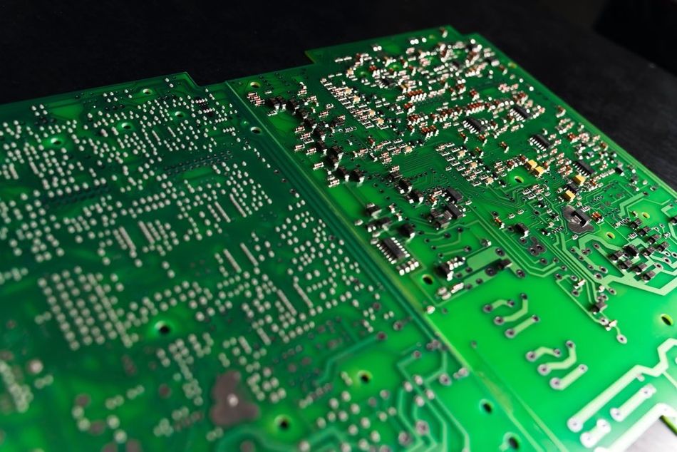
PCB Fabrication Process
The manufacturing process of a Printed Circuit Board (PCB) undergoes multiple steps to translate the design blueprint into a tangible board. Typically conducted within a specialized PCB fabrication facility, this intricate process employs various techniques such as etching, drilling, plating, and integrates Computer Numerical Control (CNC) technology for enhanced precision.
Commencing with the preparation of raw materials, usually a laminate comprising a non-conductive substrate material and a conductive copper layer, the process advances. The copper layer undergoes a series of steps: it is coated with a photosensitive film, exposed to ultraviolet light through a mask representing the circuit pattern, and subsequently developed. This exposes the circuit pattern, allowing for selective copper removal through chemical etching. The result is a circuit pattern revealed in copper, with holes drilled for through-hole components and vias, followed by plating to safeguard the copper and boost conductivity.
The culmination of the fabrication process involves the application of a solder mask, serving to shield the circuitry, prevent solder bridges, and enhance the overall robustness of the PCB. Additionally, a silkscreen layer is printed onto the board, providing essential labels and markings for component identification. Throughout these stages, CNC technology plays a pivotal role in ensuring accuracy and consistency, contributing to the high-quality production of PCBs.
Further reading: Components of a PCB: A Comprehensive Guide
Material Selection
The selection of materials for a PCB is a critical aspect of the design and fabrication processes. The choice of materials can significantly affect the final product's performance, reliability, and cost.
The most common material used for the substrate in a PCB is fiberglass-reinforced epoxy resin (FR4). FR4 provides a good balance of performance, durability, and cost. It has excellent electrical insulation properties, good thermal stability, and high mechanical strength.
The conductive layer in a PCB is typically made of copper due to its excellent electrical conductivity and ease of etching. The thickness of the copper layer can vary depending on the current-carrying requirements of the circuit. A thicker copper layer can carry more current, but it also increases the cost and complexity of the fabrication process.
Other materials used in a PCB include the solder mask, which is typically a polymer layer that protects the circuitry and prevents solder bridges, and the silkscreen, which is usually a layer of ink that provides labels and markings for the components.
The selection of materials for a PCB requires a deep understanding of the circuit's electrical, thermal, and mechanical requirements and the constraints of the fabrication process. This is a critical aspect of the PCB design and fabrication processes that can significantly affect the final product's performance, reliability, and cost.
Imaging and Etching
Imaging and etching are key steps in the PCB fabrication process, transforming the design blueprint into a physical circuit pattern on the PCB.
Imaging is the process of transferring the circuit design onto the PCB. This is typically done using a photosensitive film applied to the PCB's copper layer. The film is exposed to ultraviolet light through a mask representing the circuit pattern. The areas of the film that are exposed to the light harden, while the unexposed areas remain soft and can be washed away. This leaves a hardened image of the circuit pattern on the PCB.
Etching is the process of removing the unwanted copper from the PCB to reveal the circuit pattern. This is typically done using a chemical solution that dissolves the exposed copper. The hardened film protects the copper that forms the circuit pattern from being dissolved by the etching solution. Once the etching process is complete, the remaining film is removed, leaving behind the circuit pattern in copper.
Both imaging and etching require a high level of precision to ensure that the circuit pattern is accurately reproduced on the PCB. Any errors or defects in these processes can lead to problems in the final product's functionality. Therefore, these processes are typically carried out under controlled conditions using specialized equipment to ensure the highest level of accuracy and consistency.
Drilling and Plating
Drilling and plating are integral steps in the PCB fabrication process, contributing to the functionality and reliability of the final product.
Drilling is the process of creating holes in the PCB for through-hole components and vias. These holes allow electrical connections between different layers of the PCB. The drilling process requires a high level of precision, as the size and location of the holes can significantly affect the PCB's performance. The holes are typically drilled using computer-controlled drilling machines, which can accurately reproduce the hole pattern specified in the design blueprint.
Once the holes are drilled, the PCB undergoes a process known as plating. Plating involves depositing a thin layer of metal, typically copper, onto the surface of the PCB and inside the drilled holes. This creates a conductive path that allows electrical signals to travel between different layers of the PCB.
The plating process begins with cleaning the PCB to remove any residues from the drilling process. The PCB is then immersed in an electroplating bath containing a solution of copper ions. An electric current is passed through the solution, causing the copper ions to be deposited onto the surface of the PCB and inside the drilled holes.
The plating quality can significantly affect the PCB's performance and reliability. Poor quality plating can lead to weak or broken connections, which can cause the PCB to fail. Therefore, the plating process is closely monitored and controlled to ensure the highest level of quality and consistency.
Solder Mask and Silkscreen
In the concluding stages of the PCB fabrication process, the application of solder masks and silkscreen not only adds functional advantages but also enhances the aesthetic appeal of the final product.
Solder masks, the protective layers over the copper traces, play a crucial role in ensuring the integrity of the PCB. Firstly, they prevent solder bridges by confining solder flow to designated areas during soldering. Secondly, they provide insulation between conductive copper traces, mitigating the risk of short circuits.
Lastly, solder masks shield copper from environmental factors like moisture and oxidation, preserving the PCB's performance. Typically green and applied through a screen printing process, solder masks can adopt other colors for aesthetic reasons or to signify distinct circuit types, with black ink being a popular choice.
Silkscreen, another essential layer, involves the application of ink onto the solder mask, imparting labels and markings for components. These markings, encompassing identifiers, polarity symbols, test points, and other information, aid in PCB assembly (PCBA) and troubleshooting. While silkscreen ink is traditionally white, alternative colors may be used for contrast or aesthetic considerations. Achieving precision in the application of the silkscreen is imperative to ensure that markings are clear, accurate, and properly aligned with corresponding components.
Together, solder masks and silkscreen significantly contribute to the functionality, reliability, and user-friendliness of the PCB. Their integration demands meticulous consideration during the design phase and precise control throughout the fabrication process to guarantee the highest levels of quality and performance in the end product.
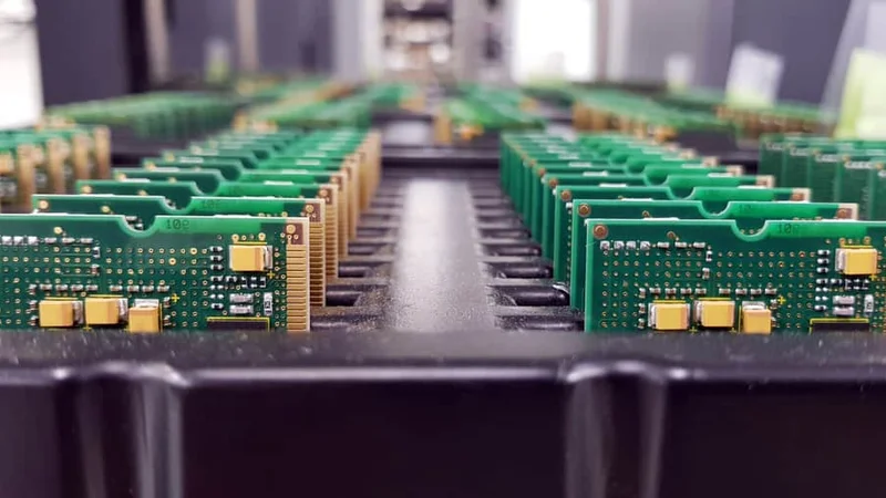
PCB Assembly Process
The PCB assembly (PCBA) process marks the stage where components are affixed to the board, transitioning it from a bare substrate into a fully operational Printed Circuit Board (PCB). This intricate process unfolds step by step, encompassing component placement, soldering, and meticulous inspection.
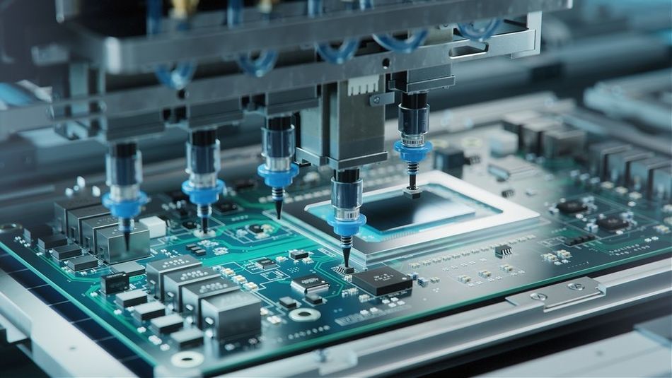
The inaugural step in this assembly dance is component placement. Following the design blueprint, automated pick-and-place machines, equipped with vacuum nozzles and precision robotic arms, delicately position components on the PCB. These machines orchestrate the arrangement, ensuring each component finds its designated spot on the board.
With components in place, the assembly progresses to the soldering stage. A metal alloy, known as solder, undergoes the transformation from solid to molten to establish a robust electrical and mechanical bond between the components and the PCB. Wave soldering caters to through-hole components, while reflow soldering caters to their surface-mount counterparts.
The grand finale of the assembly unfolds in the inspection phase. Here, a vigilant review scans the PCB for potential defects or errors, including misaligned components or subpar solder joints. Visual inspections harmonize with automated testing methods, such as in-circuit or functional testing, to ensure the final product adheres to the highest quality standards.
Throughout this orchestrated assembly, precision is paramount, with each component and connection playing a vital role in the functionality of the assembled PCB.
Component Placement
Component placement is a critical step in the PCB assembly process. It involves positioning the components on the PCB according to the design blueprint. The accuracy of component placement can significantly affect the performance and reliability of the final product.
The components are typically placed on the PCB using automated pick-and-place machines. These machines use vacuum nozzles to pick up the components from their packaging and precision robotic arms to place them in the correct locations on the PCB. The machines are programmed with the design data, which specifies each component's type, orientation, and location.
Component placement accuracy is crucial, as any misalignment can lead to problems such as poor electrical connections or short circuits. Therefore, the placement process is closely monitored and controlled to ensure the highest level of accuracy and consistency.
The speed of component placement is also important, as it can affect the production time and cost. Modern pick-and-place machines can place thousands of components per hour, making them an essential tool for high-volume PCB production. However, manual placement may be used for low-volume or prototype production, as it can be more flexible and cost-effective.
Soldering Techniques
Soldering stands as a pivotal process in the PCB assembly realm, forging the essential electrical and mechanical bonds between components and the PCB. Diverse soldering techniques are employed in PCB assembly, each presenting unique advantages and considerations that shape the manufacturing landscape.
One prevalent method for through-hole components is wave soldering. In this choreography, the PCB gracefully traverses a molten solder wave, delicately adhering to exposed metal areas to craft impeccable solder joints. Precision reigns as the height, temperature, and speed of the solder wave are adjusted to orchestrate the optimal amount of solder. Wave soldering boasts remarkable efficiency, effortlessly tending to numerous joints simultaneously. However, its dance partners are limited, as surface-mount components risk displacement in its vigorous embrace.
For the nimble-footed surface-mount components, reflow soldering takes center stage. A paste, housing solder and flux, pirouettes onto the PCB, hosting components atop. The ensemble gracefully enters a reflow oven, where the solder metamorphoses into liquid form, birthing the elegant solder joints. Temperature intricacies in the reflow process are meticulously choreographed to ensure a flawless dance, where the solder melts and solidifies with grace, forging robust and dependable joints.
In a more artisanal approach, hand soldering takes the lead, especially in low-volume or prototype productions, or when components shun the embrace of machines. A skilled hand wields a soldering iron, coaxing solder into a molten state to sculpt joints with finesse. Though demanding high skill and precision, hand soldering offers unparalleled flexibility and control, akin to a masterful solo performance.
The grandeur of each soldering technique hinges on vigilant control and monitoring, ensuring the quality of every solder joint. Lackluster soldering craftsmanship may birth feeble or undependable joints, leading the PCB towards an untimely falter. Thus, the selection of a soldering technique and the nuanced dance of soldering process parameters emerge as critical facets in the grand ballet of PCB assembly.
To enrich the performance further, the ensemble welcomes additional players, including solder mask application, printed circuit board assembly, registration holes, HASL (Hot Air Solder Leveling), hot air, inkjet, and layer alignment, each contributing its unique notes to the symphony of flawless PCB creation.
Further reading: Demystifying Soldering Techniques: A Comparison of Wave Soldering and Reflow Soldering
Inspection and Testing
Inspection and testing are crucial in the PCB assembly process, ensuring the final product's quality, functionality, and reliability.
Inspection involves visually checking the PCB for defects or errors. These can include misaligned components, poor solder joints, or physical damage. Visual inspection can be done manually by trained personnel or automated using machine vision systems. Automated Optical Inspection (AOI) systems use high-resolution cameras and image processing software to inspect the PCB for defects. These systems can detect a wide range of defects with high accuracy and speed, making them an essential tool for high-volume PCB production.
In addition to visual inspection, the PCB undergoes electrical testing to verify its functionality. Several methods of electrical testing exist, each with advantages and considerations.
In-circuit testing (ICT) involves testing the PCB by applying electrical signals and measuring the response. This can be done using a bed-of-nails tester, which uses a custom fixture with spring-loaded pins to contact specific points on the PCB. ICT can detect faults, including short circuits, open circuits, and incorrect component values. However, it requires a custom fixture for each PCB design, which can be time-consuming and costly to produce.
Functional testing similarly involves testing the PCB to see how it will be used in the final application. This can include applying power to the PCB, sending and receiving data, and monitoring the behavior of the PCB. Functional testing can provide a high level of confidence in the functionality of the PCB, but it can be complex and time-consuming to set up.
Both inspection and testing require careful planning and execution to ensure the highest level of quality and reliability in the final product. Any defects or errors detected during these processes must be addressed before the PCB can be approved.
Quality Control and Reliability
Quality control and reliability are paramount in PCB manufacturing. They ensure the final product meets the required standards and performs reliably over its intended lifespan.
Quality control involves a series of checks and tests conducted at various stages of the manufacturing process. These checks aim to detect and correct any defects or deviations from the design specifications. The checks can include visual inspection, electrical testing, and mechanical testing. The goal is to ensure that every PCB that leaves the production line meets the highest standards of quality and performance.
Reliability, on the other hand, refers to the ability of the PCB to perform consistently over time under the specified operating conditions. This is typically assessed through stress tests, subjecting the PCB to extreme conditions such as high temperatures, high humidity, and mechanical stress. The results of these tests provide an indication of how the PCB will perform over its intended lifespan.
Both quality control and reliability are critical for ensuring the performance and longevity of the PCB. They require a systematic approach and rigorous testing protocols to ensure that every PCB meets the required standards.
Quality Control Standards
Quality control standards provide a framework for ensuring the quality and reliability of PCBs. These standards specify the requirements for designing, manufacturing, and testing PCBs.
One of the most widely used standards for PCB quality control is the IPC-A-610 standard, published by the Association of Connecting Electronics Industries. This standard provides comprehensive acceptance criteria for various aspects of PCB assembly, including soldering, component placement, and cleanliness.
Another important standard is the ISO 9001 standard, which specifies the requirements for a quality management system. This standard focuses on the processes and procedures used in PCB manufacturing, requiring continuous improvement and customer satisfaction.
Compliance with these standards is typically verified through third-party audits, which assess the manufacturer's quality management system and manufacturing processes. Manufacturers who meet these standards can provide a higher level of assurance to their customers about the quality and reliability of their PCBs.
Adherence to quality control standards is a critical aspect of PCB manufacturing. It ensures that the PCBs are manufactured to a consistent level of quality, and it provides a benchmark for comparing the quality practices of different manufacturers.
Reliability Testing
Reliability testing stands as a pivotal component of quality control within the realm of PCB (Printed Circuit Board) manufacturing. Its primary objective is to evaluate the endurance and functionality of the PCB across diverse operating conditions throughout its intended lifespan.
In the domain of reliability testing, the PCB undergoes a battery of stress tests designed to simulate the extreme conditions it may encounter during its operational life. These tests encompass thermal cycling, where the PCB is subjected to repeated high and low-temperature cycles to gauge its resistance to stress. Humidity testing is another essential evaluation, exposing the PCB to elevated humidity levels to assess its resistance to moisture ingress.
Mechanical stress tests further scrutinize the PCB's robustness under physical duress. Vibrational testing involves subjecting the PCB to varying levels of vibration to evaluate its mechanical durability, while shock testing assesses its resistance to sudden impacts.
In the realm of PCB manufacturing, the incorporation of X-ray technology expands the scope of reliability tests into the electrical domain. Power cycling, a pivotal electrical stress test, subjects the PCB to repetitive cycles of powering on and off, meticulously evaluating its electrical endurance.
Concurrently, burn-in testing raises the stakes by exposing the PCB to elevated temperatures and voltages, deliberately accelerating the failure of any vulnerable components. Augmenting this orchestration, UV light joins the performance, shedding light on intricate nuances and adding depth to the comprehensive evaluation.
The outcomes of these rigorous tests, illuminated by the radiant glow of UV light, unveil a symphony of invaluable data. This data serves as a cornerstone, delineating the expected lifespan and performance of the PCB across diverse operating conditions. It becomes the virtuoso guide for manufacturers, empowering them to identify potential pitfalls and instigate refinements in both design and manufacturing processes. The radiant glow of UV light becomes a beacon, guiding manufacturers towards the pinnacle of PCB excellence and ensuring not just reliability but also the enduring longevity of their creations.
Environmental Considerations
Environmental considerations play a significant role in the PCB manufacturing process. The production of PCBs involves using various materials and chemicals, some of which can have a significant environmental impact if not managed properly.
One of the main environmental concerns in PCB manufacturing is using hazardous substances. These can include lead, mercury, and certain flame retardants, harming the environment and human health. Many manufacturers have adopted lead-free solder and other less harmful alternatives to use mitigate this.
Energy consumption is another important environmental consideration. The manufacturing process of PCBs is energy-intensive, particularly during the soldering and curing stages. Manufacturers can reduce their energy consumption by optimizing processes and using energy-efficient equipment.
Water usage is also a significant factor, as large amounts of water are used in the cleaning and rinsing stages of PCB manufacturing. Water conservation measures, such as water recycling and efficient rinsing techniques, can help to reduce water usage.
Waste Management
Waste management is a critical aspect of environmental considerations in PCB manufacturing. The process generates various types of waste, including solid waste, wastewater, and air emissions, which need to be managed properly to minimize their environmental impact.
Solid waste includes scrap PCBs and used components, which can contain hazardous substances. These wastes must be disposed of properly to prevent contamination of the environment. Many manufacturers have implemented recycling programs to recover valuable materials from their waste, such as copper and precious metals.
Wastewater is generated from the cleaning and rinsing stages of the manufacturing process. It can contain residues of solder, flux, and other chemicals, which can be harmful if released into the environment. Wastewater treatment systems remove these contaminants before the water is discharged.
Air emissions can include volatile organic compounds (VOCs) and other pollutants released during the soldering and curing stages. Air pollution control equipment, such as scrubbers and filters, capture these emissions and reduce their environmental impact.
Effective waste management requires a comprehensive approach, including waste minimization, recycling, and proper disposal. It is an essential part of the environmental responsibility of PCB manufacturers.
Sustainable Manufacturing
Within the paradigm of sustainable manufacturing in PCB production, a comprehensive approach is embraced to curtail environmental impact, bolster social responsibility, and uphold economic viability. This holistic strategy navigates the entire lifecycle of the PCB, from the sourcing of materials to the ultimate disposal or recycling of the end product.
Material selection stands out as a pivotal facet of sustainable manufacturing. The choice leans towards materials that exhibit minimal harm to the environment, exemplified by the preference for lead-free solder and halogen-free flame retardants. The adoption of recycled or recyclable materials is integral to this selection process. Take, for instance, copper, a foundational element in PCBs, where its highly recyclable nature allows for significant reduction in the environmental footprint associated with mining and refining new copper.
Copper plating, a critical stage in PCB manufacturing, also undergoes a sustainable transformation. Efforts are directed towards optimizing the process to minimize excess copper, ensuring a judicious use of this essential material. The outer layer imaging process, too, adopts sustainable practices, embracing environmentally friendly solvents and precision plotter technologies to reduce waste and enhance efficiency.
Energy efficiency emerges as another key player in sustainable manufacturing. Acknowledging the energy-intensive nature of the PCB manufacturing process, particularly during soldering and curing stages, manufacturers pivot towards optimization and the utilization of energy-efficient equipment. This not only aligns with environmental conservation but also translates into tangible cost savings.
Aiming for waste reduction takes center stage in sustainable manufacturing endeavors. Process optimization strategies are deployed to minimize waste generation, complemented by recycling initiatives and robust waste management practices. Closed-loop water systems, for instance, prove instrumental in slashing water waste by recycling and reusing water throughout the manufacturing process.
Beyond environmental considerations, sustainable manufacturing incorporates a strong thread of social responsibility. This entails championing fair labor practices, fostering safe and healthy working conditions, and embracing ethical business practices. By embracing sustainable manufacturing practices, PCB manufacturers not only diminish their environmental footprint but also actively contribute to social well-being and economic development, thus forging a path towards a more responsible and sustainable future.
Conclusion
The manufacturing of printed circuit boards (PCBs) is a complex process requiring high precision and quality control. From the initial design phase to the final inspection and testing, each step of the process plays a crucial role in determining the performance and reliability of the final product.
Environmental considerations and sustainable manufacturing practices are increasingly important in the PCB manufacturing industry. Manufacturers are adopting practices such as using less harmful materials, optimizing energy use, reducing waste, and ensuring social responsibility. These practices reduce the environmental impact of PCB manufacturing and contribute to social well-being and economic development.
Further reading: Understanding PCB Mouse Bites: A Guide to Breakaway Tabs and V-Groove Techniques
Frequently Asked Questions (FAQs)
What is the importance of inspection and testing in PCB manufacturing? Inspection and testing are crucial steps in the PCB manufacturing process. They ensure the final product meets the required standards and performs reliably over its intended lifespan. Any defects or errors detected during these processes must be addressed before the PCB can be approved.
What are some of the environmental considerations in PCB manufacturing? Environmental considerations in PCB manufacturing include using hazardous substances, energy consumption, water usage, and waste management. Manufacturers are adopting practices to mitigate these impacts, such as using less harmful materials, optimizing energy use, reducing waste, and implementing recycling programs.
What is sustainable manufacturing in the context of PCB production? Sustainable manufacturing involves implementing practices that reduce environmental impact, and enhance social responsibility, and maintain economic viability. This includes choosing less harmful materials, optimizing energy use, reducing waste, and ensuring fair labor practices.
What are some of the quality control standards in PCB manufacturing? Quality control standards provide a framework for ensuring the quality and reliability of PCBs. Some of the most widely used standards include the IPC-A-610 standard for PCB assembly and the ISO 9001 standard for quality management systems.
What is reliability testing in PCB manufacturing? Reliability testing involves subjecting the PCB to a series of stress tests to assess its performance under various operating conditions over its intended lifespan. This provides valuable data on the expected lifespan and performance of the PCB, which can be used to improve the design and manufacturing process.
References
1. Cadence. An Introduction to Printed Circuit Boards. [Cited 2023 Jan 1]. Available from: https://resources.pcb.cadence.com/blog/2022-an-introduction-to-printed-circuit-boards
2. PCBCart. PCB Manufacturing Process - A Step-by-Step Guide. 2022. [Cited 2023 Jan 1] Available from: https://www.pcbcart.com/article/content/PCB-manufacturing-process.html
3. Electronics and You. Multilayer PCB | Types of PCB. 2021. [Cited 2023 Jan 2] Available from: https://www.electronicsandyou.com/blog/multilayer-pcb.html
4. The Engineering Projects. A Detailed Guide on PCB Manufacturing Process. 2021. [Cited 2023 Jan 2] Available from: https://www.google.com/amp/s/www.theengineeringprojects.com/2021/06/a-detailed-guide-on-pcb-manufacturing-process.html/%3famp=1
5. RAYMING. Printed Circuit Board (PCB) Manufacturing Process - Printed Circuit Board Manufacturing & PCB Assembly. 2021. [Cited 2023 Jan 2] Available from: https://www.raypcb.com/pcb-board-manufacturing/
6. Creative Hi-Tech. PCB Plating: Purpose, Types, and Methods Discussed. 2022. [Cited 2023 Jan 2] Available from: https://www.creativehitech.com/blog/pcb-plating-purpose-types-and-methods-discussed/
7. Electronics Notes. PCB Manufacture: How are PCBs Made? 2021. [Cited 2023 Jan 2] Available from: https://www.electronics-notes.com/articles/constructional_techniques/printed-circuit-board-pcb/pcb-manufacturing-process.php
8. ExPlus. Printed Circuit Board (PCB) Fabrication Process and Methods. 2020. [Cited 2023 Jan 3] Available from: https://www.explus.com.tw/devices.htm#parentHorizontalTab6
9. Millennium Circuits Limited. An Ultimate Guide to the PCB Manufacturing Process. 2022. [Cited 2023 Jan 3] Available from: https://www.mclpcb.com/blog/pcb-manufacturing-process/
10. PCBWay. Electrical Test | Multi-Layer PCB Manufacturing Process. 2022. [Cited 2023 Jan 3] Available from: https://www.pcbway.com/blog/PCB_Manufacturing_Information/Electrical_Test_Multi_layer_PCB_Manufacturing_Process_15_2d72c686.html
11. WELL PCB. PCB Fabrication Process - 20 Steps Ultimate Guide on PCB Manufacturing. 2022. [Cited 2023 Jan 3] Available from: https://www.wellpcb.com/pcb-fabrication-process.html
12. PCB Power Market. PCB Manufacturing Process. 2021. [Cited 2023 Jan 3] Available from: https://www.pcbpower.com/PCB-Manufacturing-Process
13. Millennium Circuits Limited. An Ultimate Guide to the PCB Manufacturing Process. 2022. [Cited 2023 Jan 3] Available from: https://www.mclpcb.com/blog/pcb-manufacturing-process/