NAND Truth Table: A Comprehensive Guide for Digital Designers and Hardware Engineers
Understanding the full potential of the universal NAND gate by mastering its truth table, transistor implementations, electrical characteristics and real-world applications.

02 Feb, 2026. 12 minutes read
Key takeaways
The NAND truth table shows that the output is low only when all inputs are high; this inversion of the AND function makes NAND a universal building block for any digital logic circuit.
Simple RTL circuits use NPN transistors in series so that either transistor being off pulls the output high. In contrast, CMOS NAND gates use parallel PMOS transistors and series NMOS transistors to achieve low static power draw.
74LS00 TTL NAND gates operate from 4.75-5.25 V and have propagation delays of 9-15 ns, whereas modern 74HC00 CMOS NAND gates combine low power consumption with typical delays of 8 ns.
NAND flash memory arranges floating‑gate cells in series; the bit line goes low only when all word lines are high. This yields higher density and lower cost than NOR flash at the expense of slower random read access.
NAND gates form the basis of latches, multiplexers, adders and large‑scale memory devices, and their universality simplifies chip design because any logic function can be synthesized from NAND alone.
Introduction
Digital design rests on the ability to manipulate binary values reliably and predictably. Logic gates are the fundamental building blocks that make this possible, and among them, the NAND gate stands out as one of the most important. Its behaviour is summarised concisely in the NAND truth table, which describes how the gate responds to every combination of input bits. Because a NAND gate outputs a logical 1 in all cases except when all inputs are 1, it is essentially an AND gate with an inversion. This deceptively simple rule unlocks a vast range of possibilities: NAND gates are universal – with enough of them you can implement any other logic function – and they form the core of modern digital electronics from microprocessors to solid‑state drives.
This article discusses the NAND truth tables for digital design engineers, hardware engineers, and electronics students. We will discuss the foundations of logic gates, explore how the NAND function is implemented using transistors, evaluate the electrical characteristics of common logic families, and demonstrate how NAND gates can build any logic operation. The article also focuses on NAND-based sequential circuits, such as the SR latch, and examines how the NAND concept extends to non‑volatile memory.
Fundamentals of the NAND Truth Table
Basic Logic Gate Concepts
Digital systems use voltage levels to represent binary values. A logic gate is a circuit that performs a Boolean operation on its inputs to produce an output. Simple gates include NOT (inverter), AND and OR.
The truth table of a gate lists the output for every possible input combination. Understanding truth tables is crucial for designing and verifying digital circuits, as they reveal whether a circuit implements the intended logic.
The NAND gate (NOT‑AND) inverts the output of an AND gate. For inputs A and B, the Boolean expression is:

By De Morgan’s law, this can also be written as:

which highlights that the output is true if either input is false. The advantage of using NAND rather than AND and NOT separately is that NAND gates come in integrated circuits (ICs) with multiple identical gates, making them cost‑ and area‑efficient.
Suggested Reading: Understanding Logic Gate Symbols: Comprehensive Guide for Engineers
Two‑input NAND truth table
The simplest NAND gate has two inputs. Its truth table is shown alongside the standard symbol in the diagram below.
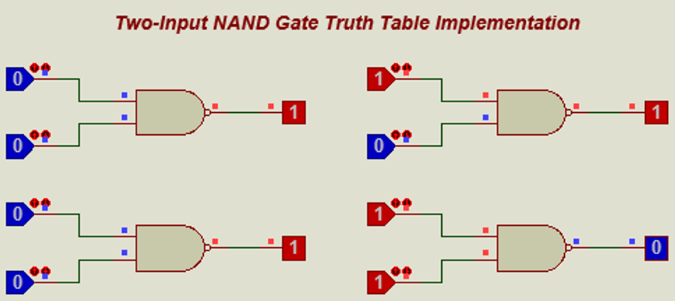
The gate outputs 1 for every combination except when both inputs are 1.
A | B | Y |
0 | 0 | 1 |
0 | 1 | 1 |
1 | 0 | 1 |
1 | 1 | 0 |
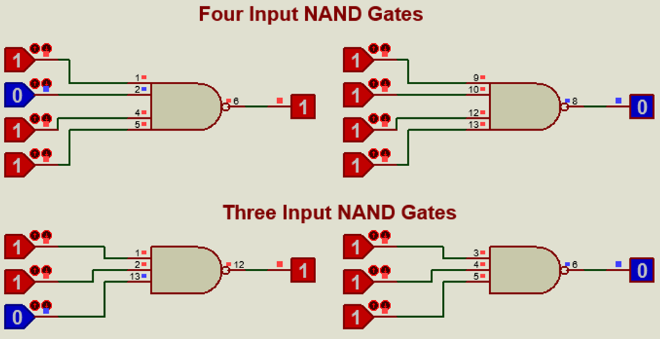
Multi‑input NAND gates
Commercial NAND ICs often provide 3‑, 4‑, or 8‑input gates to implement “all‑high” detection. The principle stays the same: the output is low only when every input is high.
For example, a three‑input NAND gate uses the expression:

Likewise, A four-input NAND gate works on the following logic:

As the number of inputs increases, the NAND truth table grows exponentially, but the pattern remains simple: a single 0 on any input forces the output high. Multi‑input NAND gates are used in decoders, parity checkers, and combinational circuits that need to detect a specific binary pattern.
Transistor‑Level Implementations
Understanding how NAND behaviour arises from transistor arrangements provides valuable insight into propagation delay, power consumption, and noise immunity. There are three primary ways to realise a NAND gate: resistor–transistor logic (RTL), transistor–transistor logic (TTL), and complementary metal‑oxide‑semiconductor (CMOS) logic.
RTL NAND: series NPN transistors
A basic two‑input NAND gate can be built using two NPN transistors connected in series with a pull‑up resistor, as shown below:
The collectors of the transistors connect to a positive supply via a resistor.
The emitters are connected to ground.
Inputs A and B drive the transistor bases.
Recommended Reading: Transistor as a Switch: Theory and Practical Implementation for Digital and Hardware Engineers
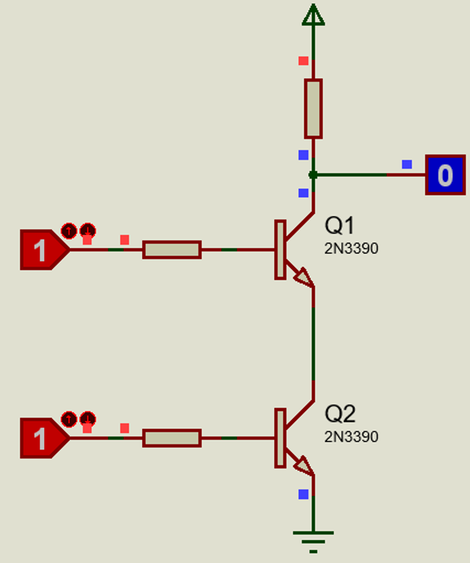
This configuration ensures that the output node is pulled high through the resistor whenever either transistor is off. Only when both base inputs are high (turning both transistors on) does current flow through the series path, pulling the output low. The truth table mirrors the NAND behaviour:
A | B | Q1 state | Q2 state | Output (Y) |
0 | 0 | Off | Off | 1 |
0 | 1 | Off | On | 1 |
1 | 0 | On | Off | 1 |
1 | 1 | On | On | 0 |
While RTL gates are simple, they suffer from slow switching and high static power consumption because the pull‑up resistor is always conducting current when the output is low.
Recommended Reading: RTL Design: A Comprehensive Guide to Understanding and Implementing Register-Transfer Level Design
TTL NAND: multi‑emitter transistors and active pull‑ups
Transistor–transistor logic uses bipolar junction transistors (BJTs) in a more complex arrangement to improve speed and reduce power. In a 74LS00 quadruple NAND gate IC, each two‑input gate uses a multi‑emitter NPN transistor to perform the AND function and a totem‑pole output stage for inversion and drive capability.
According to the Texas Instruments datasheet, SN74LS00 devices operate with a supply voltage between 4.75 and 5.25 V. The high‑level input threshold is around 2 V, and the low‑level threshold is 0.8 V.
CMOS NAND: Parallel PMOS and Series NMOS transistors
Complementary MOS technology achieves NAND functionality with two p‑channel MOSFETs (PMOS) in parallel between the supply and the output and two n‑channel MOSFETs (NMOS) in series between the output and ground.
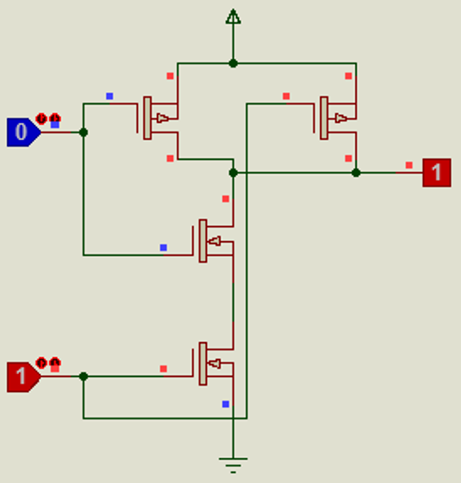
When either input is low, at least one PMOS transistor is on and at least one NMOS is off, so the output is pulled high. Only when both inputs are high do both NMOS devices conduct, pulling the output low. Because CMOS gates only draw significant current during switching, they exhibit very low quiescent power consumption.
Suggested Reading: The Designers Guide to MOSFET and GaN FET Applications
Comparing TTL and CMOS NAND
Feature | TTL NAND (74LS00) | CMOS NAND (74HC00) |
Logic family technology | Bipolar junction transistors (BJTs) | Complementary MOS (NMOS + PMOS) |
Supply voltage | 4.75–5.25 V | 2–6 V |
Typical propagation delay | 9–10 ns | 8–9 ns |
Static power consumption | Continuous current draw | Very low (only during switching) |
Noise immunity | Medium–high; defined thresholds | High; wide noise margins |
Fan‑out | 10–20 inputs (depends on variant) | 10 LS‑TTL loads |
Typical applications | Legacy digital circuits, glue logic | Modern microcontrollers, low‑power devices |
Universal Gate and Logic Synthesis with NAND
Why NAND gates are universal
A gate is universal if any Boolean function can be constructed solely from that gate type. The NAND gate satisfies this criterion because it combines inversion and conjunction. By strategically connecting inputs and outputs, designers can emulate all other basic gates.
This universality simplifies manufacturing; many complex integrated circuits, including microprocessors and memory arrays, use NAND as their core building block.
Building Basic Gates from NAND
Below are the standard configurations for synthesising NOT, AND and OR gates using only NAND gates. These constructions follow directly from the definition of NAND and De Morgan’s law:
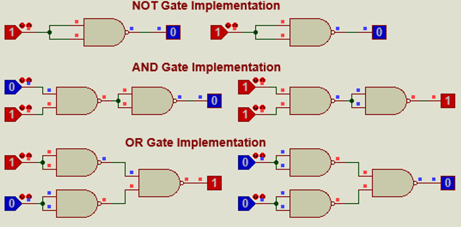
More complex functions like XOR and multiplexers can also be built using networks of NAND gates. Because NAND is universal, chip designers often standardise on it to streamline fabrication and ensure consistent delay across logic blocks.
Sequential Circuits with NAND Gates
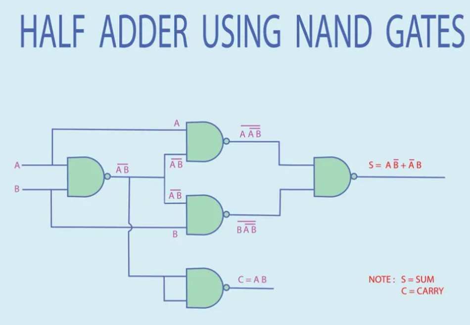
The universality of NAND extends beyond combinational circuits. Flip‑flops and latches also utilise NAND structures. A basic example is the SR latch constructed from two cross‑coupled NAND gates. Unlike the NOR‑based SR latch, this version accepts active‑low inputs (labelled S’ and R′). The truth table is as follows:
S' | R' | Q (output) | Q’‾ | Description |
1 | 1 | Latches previous state | Complement | No change |
0 | 1 | 1 | 0 | Set state |
1 | 0 | 0 | 1 | Reset state |
0 | 0 | Undefined | Undefined | Forbidden (both outputs forced high) |
In TTL and CMOS datasheets, the typical propagation delay of the NAND gates determines how quickly the latch responds to input changes; for example, the 74HC00 has delays around 9–15 ns. Designers must ensure that setup and hold times of the latch are met, and care should be taken to avoid the illegal condition (both inputs low), which causes metastability.
More advanced sequential circuits like JK flip‑flops, D flip‑flops, counters and shift registers can all be built from NAND gates, either directly or by first synthesising other gate types. NAND latches are commonly used for switch debouncing and basic memory storage in TTL logic families.
Suggested Reading: Mastering Flip-Flop Circuits: Theory, Design, Types, and Real-World Applications
Electrical Characteristics and Design Considerations
Threshold Voltages and Noise Margins
For reliable operation, inputs and outputs must meet the specified voltage levels. In TTL logic, a high-level input VIH is typically ≥ 2 V, and a low-level input VIL is ≤ 0.8 V. CMOS thresholds scale with the supply voltage: for a 74HC00 at 4.5 V, VIH ≈ 3.15 V and VIL ≈ 1.35 V.
These thresholds define the noise margins, the allowable deviation from ideal logic levels before the gate misinterprets a signal. CMOS typically offers wider noise margins than TTL, making it less susceptible to interference.
Fan‑in and Fan‑Out
The fan‑in of a gate is the number of inputs it accepts. TTL NAND gates come in dual, triple, quadruple and octal configurations; unused inputs should be tied to logic high through a resistor to prevent noise coupling.
Fan‑out refers to the number of gate inputs that a single output can drive. The 74HC00 can drive 10 LS‑TTL loads. Exceeding fan‑out degrades rise and fall times and increases propagation delay due to capacitive loading.
Propagation Delay
Propagation delay is the time it takes for a change at an input to affect the output. Under typical conditions (Vcc = 5V, Cl = 15pF), a 74LS00 shows a propagation time ≈ 9 ns to 10 ns. The 74HC00 has similar typical delays around 8–9 ns, with a maximum of 15 ns over temperature.
Power Consumption
TTL gates draw static current whenever inputs or outputs are at certain logic levels; thus total power consumption is proportional to the number of gates and how often they switch. CMOS gates consume power mainly during switching as they charge and discharge internal capacitances.
For a 74HC00, quiescent current is ≤ 20 µA. Reducing the supply voltage and operating frequency further decreases power. However, CMOS gates are more susceptible to latch‑up if input voltages exceed supply rails; proper input protection and ESD measures are essential.
Interfacing TTL and CMOS
When mixing logic families, designers must pay attention to voltage levels and current capabilities. HCT (High‑speed CMOS, TTL‑compatible) devices have CMOS internals but TTL‑level input thresholds, allowing direct interfacing with TTL outputs. Alternatively, small resistor networks or level‑shifting ICs can adapt voltage levels.
NAND in Memory Technology
From logic gate to flash cell
The NAND gate’s truth table is more than a logic curiosity – it inspired the architecture of NAND flash memory. Flash memory stores data in floating‑gate MOSFETs, which maintain their charge (and hence logic state) even when power is removed. In NAND flash, cells are connected in series to a bit line. The chain acts like a NAND logic function: the bit line will see a low voltage only when all word lines in the series string are high, analogous to the NAND truth table.
In contrast, NOR flash arranges cells in parallel, allowing random access to individual bits but requiring more area. Because of the series connection, NAND flash achieves higher density and lower cost per bit than NOR. The physical design of NAND flash cells allows roughly 40 % less area than NOR flash.
However, NOR flash has faster read times because each bit can be accessed directly. NAND flash reads and writes operate on pages and blocks, which are slower to access randomly but faster for bulk operations.
Suggested Reading: HBM Memory: Complete Engineering Guide & Design Optimization 2025
Cell operation
Each NAND flash cell contains a floating gate that can be charged or discharged via Fowler–Nordheim tunnelling. When the floating gate holds charge, it raises the threshold voltage of the transistor, representing a stored 0; when discharged, the threshold is low, representing a 1. T
o program or erase data, high voltages are applied to the word lines to transfer electrons through the insulating layer. Because cells are wired in series, reading or programming a particular cell involves enabling all transistors in its string.
Applications of NAND Flash Memory
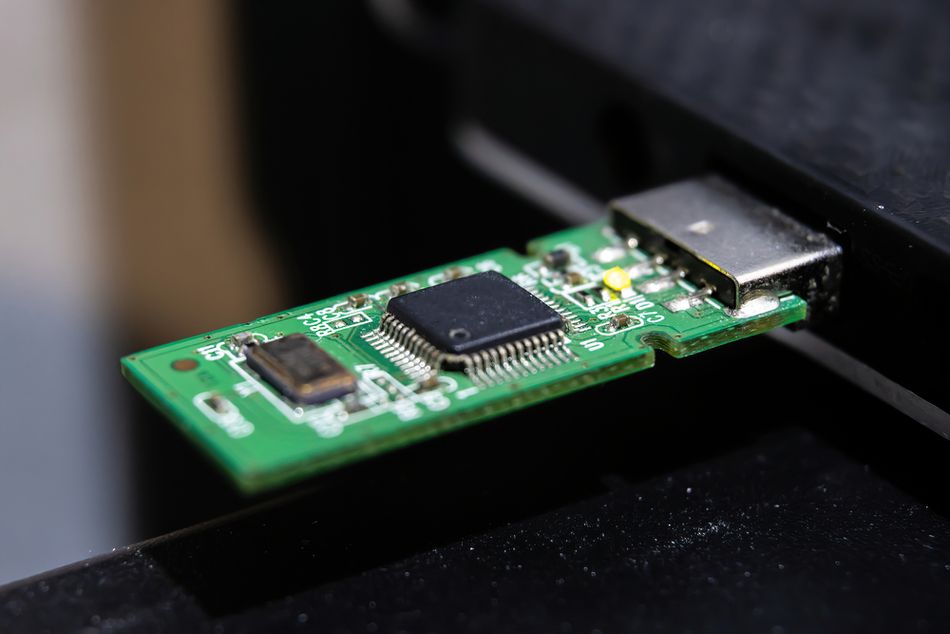
NAND flash’s high density and low cost make it ubiquitous in solid‑state drives (SSDs), USB flash drives, memory cards, smartphones and embedded storage. NOR flash, with its faster random reads and high reliability, is used for firmware storage in microcontrollers, BIOS chips and boot ROMs. Many embedded systems use both: a small NOR chip for boot code and a large NAND array for file storage.
Practical Applications of NAND Gates
The universality and efficiency of NAND gates mean they appear in countless digital designs. Here are some common applications:
Decoders and encoders: Multi‑input NAND gates detect specific patterns of bits and are used to build address decoders for memory modules, chip select circuits and instruction decoding.
Multiplexers/demultiplexers: Combining NAND gates with inverters and wiring allows the selection or distribution of data lines based on control signals. For example, a 2:1 multiplexer can be built using four NAND gates.
Arithmetic logic units (ALUs): NAND gates form fundamental logic blocks for adders, subtractors and comparators. Carry generation and propagation networks often rely on NAND and NOR trees because of their speed and compactness.
Error detection: Parity generators/checkers use cascaded NAND gates to implement XOR functions, providing simple error‑checking in communication protocols.
Sequential logic: Latches, flip‑flops, shift registers and counters often use NAND gates in their core feedback loops, as described earlier.
Microprocessor design: Many CPU building blocks, such as instruction decoders, control logic and micro‑operations, are implemented using dense networks of NAND and NOR gates. Because NAND is universal, designers can standardise cell libraries around it to simplify design and verification flows.
Suggested Reading: How is a Microprocessor Different from an Integrated Circuit?
Future Trends and Innovations
The basic NAND gate has not changed since its invention, but the contexts in which it is used continue to evolve. Two major trends are reshaping how NAND truth tables impact modern technology:
3D and multi‑level NAND Flash
Manufacturers are pushing the limits of storage density by stacking NAND strings vertically and storing more bits per cell. Vertical 3D NAND architectures connect series strings through vertical vias, enabling terabit‑scale chips.
Quantum and beyond‑CMOS logic
Research into quantum computing and emerging technologies like spintronics or memristive devices may supplant traditional CMOS, but classical logic gates remain important for interfacing with periphery and control circuits. NAND will likely continue to serve as a universal gate in hybrid systems, bridging quantum or neuromorphic cores with classical control electronics.
Programmable logic and FPGAs
Field‑programmable gate arrays are built from look‑up tables (LUTs) that can implement any logic function, but at their heart, they often map functions to LUTs configured as NAND and NOR gates. Modern synthesis tools optimise logic into NAND and NOR to minimise area and delay. For engineers familiar with NAND truth tables, understanding how synthesis maps high‑level descriptions to gate‑level implementations is essential.
Suggested Reading: FPGA Architecture: A Comprehensive Guide for Digital Design Engineers
Conclusion
The NAND gate simplifies digital logic by inverting the output of an AND gate, it becomes a universal building block. The NAND truth table reveals that a single 0 on any input forces the output high, a property that underpins applications from combinational logic to high‑density memory. Engineers use NAND gates in diverse forms – from RTL circuits and TTL ICs to modern CMOS and advanced 3D NAND flash – each with trade‑offs in speed, power and reliability. Understanding the transistor implementations, electrical characteristics and synthesis techniques discussed here equips designers to harness the full potential of this versatile gate.
FAQs
1. What combination of inputs makes a NAND gate output low?
A NAND gate outputs logic 0 only when all of its inputs are at logic 1. If any input is 0, the output remains 1. This principle holds for two‑input, three‑input and larger NAND gates.
2. What is the difference between TTL and CMOS NAND gates?
TTL NAND gates (e.g., 74LS00) use BJTs, operate at 5 V and have propagation delays around 9–15 ns. They draw a constant current even when idle. CMOS NAND gates (e.g., 74HC00) use MOSFETs, support supply voltages from 2–6 V and have similar or better propagation delays with much lower static power consumption.
3. Why are NAND gates called universal gates?
NAND gates can implement any Boolean function by combining multiple NANDs. By tying inputs together they behave as inverters, and by cascading stages you can create AND, OR, XOR and more. This universality allows designers to build entire digital systems using a single gate type, simplifying manufacturing and design.
4. How does NAND flash differ from NOR flash memory?
NAND flash arranges floating‑gate cells in series, reducing the number of bit lines and achieving higher storage density and lower cost per bit. NOR flash connects cells in parallel, allowing random access and faster read speeds but at a higher cost and lower density. NAND is ideal for bulk storage such as SSDs and USB drives, while NOR is used for firmware and boot code.
5. What is the typical endurance of NAND flash memory?
NAND flash cells endure approximately 50 000–100 000 program/erase cycles before wear degrades their reliability. Endurance can be increased through error‑correcting codes and wear‑levelling algorithms. NOR flash typically offers higher endurance and data retention.
6. Can NAND gates be used to build memory elements?
Yes. Cross‑coupled NAND gates form SR latches, the simplest form of static memory. More complex flip‑flops, registers and RAM cells are built from NAND and NOR structures combined with transmission gates and pass transistors. NAND’s universal property ensures that any sequential logic can be built from it.
7. How do propagation delays affect timing in large circuits?
Each NAND gate introduces a finite propagation delay. Cascading gates adds their delays, so long combinational paths can violate setup and hold times in synchronous systems. Using faster logic families (e.g., Schottky TTL or advanced CMOS), reducing capacitive loading and pipelining logic stages help meet timing requirements.
References
“Logic NAND Gates: A Comprehensive Tutorial,” TheLinuxCode. [Online]. Available: https://thelinuxcode.com/logic-nand-gate-tutorial/
“TTL Logic family | Digital Logic Families,” Electronics Tutorial. [Online]. Available: https://www.electronics-tutorial.net/digital-logic-families/ttl-logic/
“Transistor Transistor Logic (TTL) - Circuit diagram, Characteristics, Truth Table, Advantages and Disadvantages,” poriyaan.in. [Online]. Available: https://eee.poriyaan.in/topic/transistor-transistor-logic--ttl--11601/
“SN74LS00 data sheet, product information and support,” Texas Instruments. [Online]. Available: https://www.ti.com/product/SN74LS00
“Logic gates applications,” schoolphysics. [Online]. Available: https://www.schoolphysics.co.uk/age16-19/Electronics/Logic%20gates/text/Logic_gates_applications/index.html
“Nand Gates Future Forecasts: Insights and Trends to 2034,” ReportPinnacle. [Online]. Available: https://www.reportpinnacle.com/reports/nand-gates-58880
G. Author et al., “Electrical Characterization of Integrated 2-Input TTL NAND Gate at Elevated Temperature, Fabricated in Bipolar SiC-Technology,” Mater. Sci. Forum, vol. 924, pp. 958–961, 2020. [Online]. Available: https://www.scientific.net/MSF.924.958.pdf
in this article
1. Introduction2. Fundamentals of the NAND Truth Table3. Transistor‑Level Implementations4. Universal Gate and Logic Synthesis with NAND5. Electrical Characteristics and Design Considerations6. NAND in Memory Technology7. Practical Applications of NAND Gates8. Future Trends and Innovations9. Conclusion10. FAQs11. References