Half Adder Circuit—Theory, Design, and Implementation
A comprehensive guide to half adder circuits for engineers and technical learners. Learn the theory behind half adders, explore truth tables, logic expressions, K maps, implementations with Logic gates, TTL/CMOS ICs, Verilog modelling, propagation delays, design strategies, and applications.

27 Nov, 2025. 11 minutes read
Key takeaways
A half adder is a fundamental combinational logic circuit that adds two single‑bit binary numbers (A and B) and produces a Sum (S) and Carry (C) output. It uses an XOR gate for the sum and an AND gate for the carry bit.
The half adder truth table lists all input combinations and corresponding sum and carry outputs. The Boolean expressions for the outputs are S = A ⊕ B and C = A · B. Karnaugh‑map minimization yields the same expressions.
You can implement a half adder using XOR and AND gates, universal NAND gates, or NOR gates. Practical implementations on breadboards use TTL ICs such as 74LS86 (quad XOR) and 74LS08 (quad AND).
Half adder circuits must account for propagation delay, power consumption, and fan‑out. In the 74xx family, high‑speed CMOS (74HC) logic has lower power consumption and similar or slightly faster propagation delays than low‑power Schottky (74LS), while advanced CMOS (74AC) is much faster (e.g., typical 74xx00 NAND gate delays of 16/10 ns for 74LS, 16/8 ns for 74HC, and 6.5/4.5 ns for 74AC).
Half adders are used in arithmetic circuits, digital signal processing, address decoding, encoders/decoders, multiplexers/demultiplexers, and counters. They serve as building blocks for full adders, ripple‑carry adders, and arithmetic logic units (ALUs)
Introduction
Binary arithmetic lies at the heart of digital design. Adding two binary digits is the simplest arithmetic operation and forms the basis for more complex functions such as multiplication, division, and address calculation. The half adder circuit performs the addition of two single‑bit numbers without considering any incoming carry from a previous stage. Although simple, understanding half adder circuits is essential for digital design engineers, hardware engineers, and electronics students because these circuits form the foundation of full adders, ripple‑carry adders, and arithmetic logic units.
This article provides an in‑depth examination of half adder circuits, starting with theoretical concepts (truth tables, Boolean expressions, Karnaugh maps) and progressing to practical implementation with logic gates, TTL/CMOS ICs, and hardware description languages. We also discuss design considerations such as propagation delay and power consumption, explore advanced low‑power techniques, and outline applications in modern digital systems.
Suggested Reading: Comprehensive Guide to 4-bit Adders: Theory, Implementation and Modern Innovations
The Importance of Half Adders
While full adders and more complex arithmetic units perform most real‑world computations, half adders remain important for theoretical understanding of adder cirucits because:
Half adders provide the foundation for multi‑bit addition. Full adders can be constructed by connecting two half adders and adding an OR gate for the carry outputs. Understanding half adders is therefore essential for understanding full adders and ripple‑carry adders.
Half adders are the building blocks for digital circuits. They are used in data processing, address decoding, encoders, decoders, multiplexers, demultiplexers, and counters.
They provide educational value because the simplicity of a half adder makes it an ideal starting point for learning Boolean algebra, logic gate design, and Karnaugh‑map minimization.
Fundamentals of Half adder circuits
Truth table and Boolean expressions
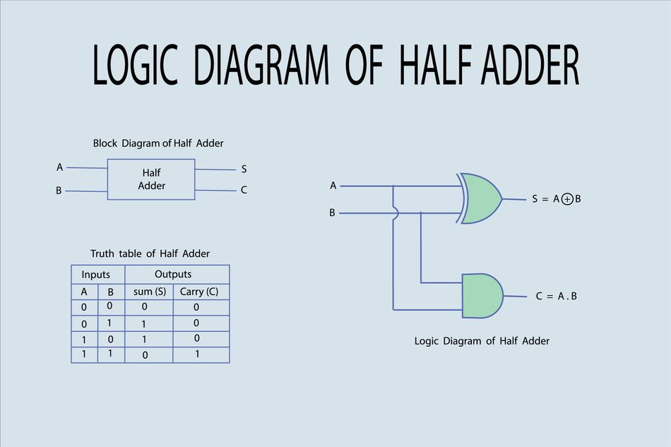
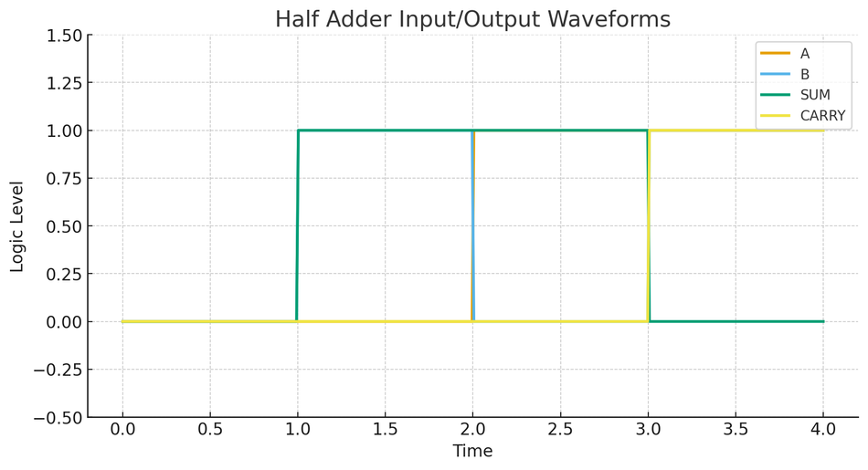
A half adder has two binary inputs (A and B) and two binary outputs: Sum (S) and Carry (C). The circuit adds the input bits and produces the sum and carry bits. The truth table is shown below
| Input (A) | Input (B) | Sum (S) | Carry (C) |
| 0 | 0 | 0 | 0 |
| 0 | 1 | 1 | 0 |
| 1 | 0 | 1 | 0 |
| 1 | 1 | 0 | 1 |
The truth table shows four possible input combinations. The output Sum corresponds to the least significant bit of the binary sum, while Carry indicates an overflow into the next higher bit. The Boolean expressions derived from the truth table (and confirmed via Karnaugh‑map minimization) are:
S = A ⊕ B and C = A ⋅ B
These expressions imply that the Sum is high only when exactly one of the inputs is high, and the Carry is high only when both inputs are high.
Logic‑Gate Implementation of Half Adders
A straightforward half‑adder implementation uses one XOR gate for the sum and one AND gate for the carry. Figure 1 features both gates receiving the same inputs, A and B, and generating outputs S and C.
In hardware, the half adder can be realized using discrete logic ICs. Two common TTL chips are the 74LS86 (quad XOR) and the 74LS08 (quad AND).
Implementation using universal gates
NAND‑only half adder
Because NAND is a universal gate, any logic circuit can be implemented using only NAND gates. Such a half adder requires at least five NAND gates.
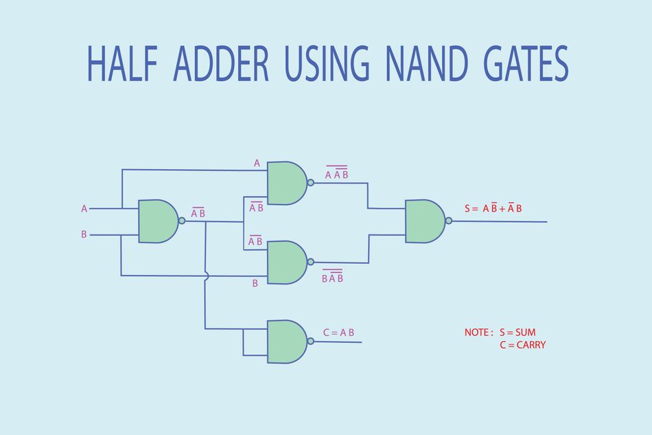
The first NAND gate receives inputs A and B. The output of this gate feeds three additional NAND gates, along with the original inputs
Two of these gates produce intermediate results that feed a final NAND gate producing the Sum.
The third gate directly produces the Carry. The resulting equations simplify to the standard equation for half adders as discussed earlier.
While NAND implementation uses more gates and brings about extra propagation delay, it’s useful as it simplifies hardware design. It’s ideal for integrated designs that only provide NAND logic or when cost optimization favors using a single type of gate.
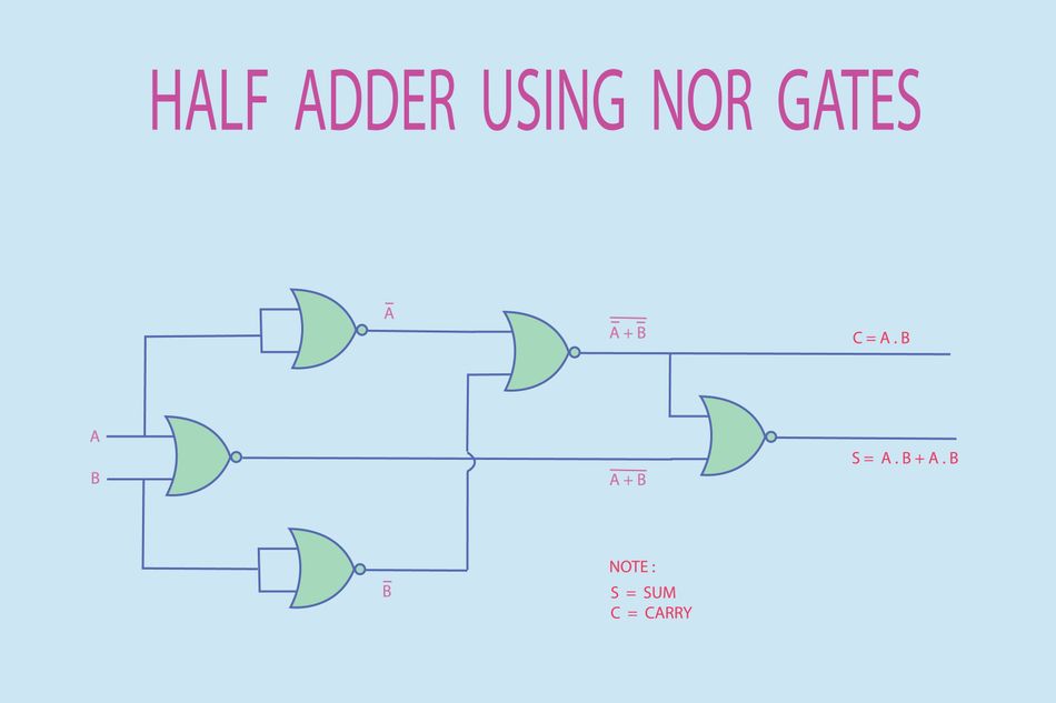
NOR‑only half adder
NOR is also a universal gate, so the half adder can be implemented using only NOR gates. Similar to the NAND‑based design, the NOR implementation uses five gates. The Sum bit is produced by combining inverted inputs, and the Carry bit is generated through additional NOR combinations.
Half Adder using CMOS and pass‑transistor logic
In CMOS technology, logic gates are constructed from complementary pairs of p‑channel and n‑channel MOSFETs. A standard CMOS XOR gate typically uses eight to twelve transistors, while an AND gate requires six transistors. However, there are alternative logic styles that can reduce transistor count and power consumption:
Pass‑Transistor Logic (PTL): PTL implements logic functions using transistors that pass signals based on control inputs. Research suggests that pass‑transistor logic can reduce transistor count but suffers from voltage‑drop issues. Combining NMOS and PMOS devices in transmission gates alleviates this problem.
Suggested Reading: MOSFET Symbol: Theory, Practical Usage and Future TrendsGate Diffusion Input (GDI) and Modified GDI (MGDI): GDI introduces a design cell that reduces transistor count by allowing input gating at the source and gate of MOSFETs. MGDI further modifies the technique to minimize delay and power. According to research, half adder and full adder circuits using MGDI with Zipper Logic achieve lower power consumption, improved speed, and noise immunity compared with conventional CMOS designs.
Propagation Delay and logic families
Propagation delay is the time between a change at the inputs of a gate and the corresponding change at the output. In multi‑gate circuits like adders, accumulated delays determine the maximum clock frequency. Within the 74xx logic family, three sub‑families are commonly used:
Family | Technology | Typical propagation delay (74xx00 NAND) | Characteristics | Application notes |
74LS | Low‑power Schottky TTL | 16 ns max / 10 ns typical | Moderate power consumption, good fan‑out, widely available | Suitable for medium‑speed designs (≤ 5 MHz), less static‑sensitive |
74HC | High‑speed CMOS | 16 ns max / 8 ns typical | Lower power consumption than LS, slightly faster or comparable speed | Works at lower supply voltages, high input impedance; good for battery‑powered systems |
74AC | Advanced CMOS | 6.5 ns max / 4.5 ns typical | Very low propagation delay, higher speed and drive strength | Suitable for high‑speed adders and ALUs; requires careful signal integrity design |
Digital designers must consider propagation delay when cascading half adders into full adders or ripple‑carry adders. The delay of a full adder using two XOR gates and an AND/OR combination is approximately twice the XOR gate delay plus the delay of the carry logic.
Power Consumption
Power consumption depends on switching activity, capacitance, supply voltage, and technology.
In TTL logic, static power is consumed because pull‑up resistors or transistor bias currents draw current even when the output is idle.
CMOS logic significantly reduces static power consumption because current flows only during switching events. High‑speed CMOS (74HC), therefore, offers both speed and low power consumption, making it preferable to 74LS for many applications.
In advanced VLSI designs, MGDI and Zipper Logic offer further power savings by minimizing transistor count and switching events. Engineers designing portable or battery‑powered devices should evaluate these techniques when implementing arithmetic units.
Suggested Reading: Inside the next generation of efficient and compact power management
Half adder in HDL (Verilog)
Hardware description languages allow designers to describe circuits at different abstraction levels and synthesize them into hardware. The following code provides a Verilog implementation of a half adder using structural, dataflow, and behavioral modelling. The structural version instantiates XOR and AND gate modules:
module half_adder_structural (
    input  a,
    input  b,
    output s,
    output c
);
  xor gate_xor (s, a, b);    // XOR gate for sum
  and gate_and (c, a, b);    // AND gate for carry
endmodule
The dataflow version uses continuous assignment statements:
module half_adder_dataflow (
    input  a,
    input  b,
    output s,
    output c
);
  assign s = a ^ b;   // XOR for sum
  assign c = a & b;   // AND for carry
endmodule
The behavioral model uses an always block to model combinational logic using procedural assignments. Designing testbenches to verify half adder modules ensures correct synthesis and simulation.
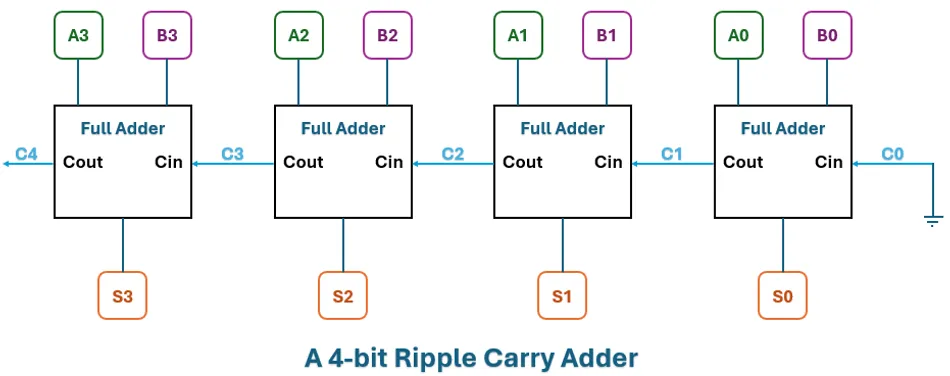
In a full adder, two half adders can be cascaded by connecting the sum output of the first half adder to one input of the second and combining the carry outputs through an OR gate.
Suggested Reading: Verilog vs VHDL: A Comprehensive Comparison
Applications of half adders
Half adders serve as fundamental building blocks for many digital circuits:
Arithmetic circuits: Multi‑bit adders and subtractors rely on half adders and full adders to perform binary addition. Two half adders and an OR gate form a full adder. Ripple‑carry adders cascade full adders to create adders of arbitrary width. Carry‑lookahead adders improve speed by computing propagate and generate signals; the basic propagate (P) and generate (G) functions correspond to the sum and carry of a half adder.
Data processing: Half adders appear in digital signal processors, encryption hardware, parity generators, and arithmetic logic units (ALUs). They also participate in multiplication circuits as part of partial product accumulation.
Address decoding: Memory addressing uses half adders in address‑decoding logic to compute intermediate bits.
Encoders/decoders: In digital communication systems, half adders help implement encoder and decoder circuits for error detection and correction.
Multiplexers/demultiplexers: Half adders assist in selecting and routing data lines in multiplexers and demultiplexers.
Counters: Binary counters use half adders to increment the least significant bit and propagate carries to higher bits.
Design Trade‑offs and Best Practices
Choosing between Half adders and Full adders
Half adders are insufficient when there is a carry input from a previous stage, which is almost always the case in multi‑bit addition. Therefore, full adders are used in cascades.
However, half adders are still used in the least significant stage or in circuits where no carry‑in is present (e.g., parity bit generation, half subtractors). When designing arithmetic units, consider using half adders for the LSB and full adders for the remaining bits.
Propagation Delay vs. Gate Count
Using XOR and AND gates yields minimal propagation delay because the sum and carry outputs appear after one gate delay each. Implementations using NAND or NOR gates require additional gate levels, increasing propagation delay.
In high‑speed designs, prioritize direct XOR/AND implementations or parallel carry‑lookahead architectures. For cost‑sensitive designs, using uniform gate types (e.g., NAND) may reduce manufacturing complexity but at the expense of speed.
Logic Family Selection
The choice of logic family impacts speed, power, and noise margins: The following table summarizes the applications and suitable logic families:
Purpose | Logic Family | Advantage |
Prototyping and experiments | 74LS series TTL chips | Widely available and cost friendly |
Low-Power Applications | 74HC CMOS chips | Offer low static power consumption |
High-Speed Applications | 74AC series chips or dedicated CMOS XOR/AND Gates | Minimal propagation delay |
VLSI Design | MGDI or Pass-transistor logic | Reduced transistor count and low power consumption |
Fan‑in and fan‑out
Designers must ensure that gate outputs can drive the inputs of subsequent gates. TTL and CMOS logic have different fan‑out ratings (number of inputs a gate can drive) and input capacitance.
When cascading half adders, verify that the total load does not exceed the driving capability. Buffering or using logic families with higher drive strength (e.g., 74AC) may be required.
Noise immunity and voltage levels
TTL logic levels differ from CMOS logic levels (e.g., TTL high threshold is ~2 V, CMOS high threshold is ~0.7 * VCC).
When interfacing TTL half adders (74LS) with CMOS devices, use level‑shifting or choose mixed‑logic families such as 74HCT that provide TTL‑compatible input thresholds.
Power‑Supply decoupling
ICs, especially CMOS devices, require proper decoupling capacitors (e.g., 0.1 µF ceramic capacitors across VCC and ground) placed near the IC pins to suppress voltage spikes caused by switching currents. Without decoupling, the circuit may experience logic errors due to supply noise.
Suggested Reading: Decoupling Capacitors: Mastering Power Integrity in Electronic Design
Low‑power design strategies
In low‑power designs, minimize switching events and capacitance:
Use high‑speed CMOS or MGDI: These families reduce static and dynamic power consumption.
Minimize glitching: Avoid unnecessary toggling by carefully arranging gates and using gating signals.
Clock gating: In synchronous systems, disable unused portions of the circuit to prevent unnecessary switching.
Verification and Testing
Always verify designs through simulation and hardware testing. For Verilog designs, use testbenches to apply all input combinations and observe outputs.
Hardware prototypes should be tested under worst‑case conditions (temperature, supply voltage variations) to ensure reliability.
Future Directions and Advanced Topics
Quantum and reversible half adders
In emerging quantum computing and reversible logic, adder circuits must be reversible (no information loss) to comply with quantum coherence and thermodynamic requirements. Reversible half adders implement sum and carry outputs along with additional outputs to preserve reversibility.
Ternary and multi‑valued half adders
While the binary half adder processes two discrete input states, researchers explore ternary (three‑valued) logic circuits. A ternary half adder would have three input states and different sum and carry output codes.
Balanced ternary half adders show promise for efficient arithmetic in certain computing architectures, though they require non‑standard logic devices.
AI and hardware acceleration
Machine learning accelerators implement specialized arithmetic units, such as fused multiply‑add (FMA) units, to improve energy efficiency. Although these units involve complex operations, they are built from simple building blocks like half adders and full adders.
Recommended Reading: Designing Energy-Efficient AI Accelerators for Data Centers and the Intelligent Edge
Conclusion
Half adders play a fundamental role in digital electronics. They are quite simple to design, yet they are inevitable building blocks for full adders, counters, encoders, and arithmetic logic units. Understanding the truth table, Boolean expressions, and various implementation techniques empowers engineers and students to design reliable and efficient combinational logic circuits.
The key takeaway is that a half adder adds two single‑bit inputs to produce a sum and carry output using an XOR gate and an AND gate. Implementation options range from TTL and CMOS logic gates to universal NAND or NOR gate realizations, as well as advanced transistor‑level techniques like MGDI. Practical considerations—propagation delay, power consumption, logic family selection, and fan‑out—drive design decisions. In an era of rapid technological advancement, mastering these basic circuits ensures a solid foundation for understanding and innovating in digital systems.
FAQs
1. What is the difference between a half adder and a full adder?
A half adder adds two single‑bit numbers and produces a sum and carry. It cannot process a carry input. A full adder adds three bits—typically two operands and a carry‑in from a previous stage—and produces a sum and carry‑out. Two half adders and an OR gate can be combined to form a full adder.
2. Why can’t a half adder be used alone for multi‑bit addition?
In multi‑bit binary addition, each bit may produce a carry that must be added to the next higher bit. Because a half adder lacks a carry input, it cannot incorporate this incoming carry; thus full adders are required for all but the least significant bit.
3. Which logic gates are used in a half adder?
The minimal half adder uses one XOR gate for the sum and one AND gate for the carry. Universal implementations using only NAND or only NOR gates are also possible, requiring at least five gates.
4. What are the advantages of using CMOS over TTL for half adder circuits?
CMOS logic (e.g., 74HC and 74AC) consumes less static power and generally offers equal or lower propagation delays than TTL. CMOS also supports a wider supply voltage range. However, CMOS inputs are sensitive to static discharge and require proper handling.
5. How do propagation delays affect adder performance?
Each logic gate introduces a delay. In a half adder, the sum and carry outputs appear after one gate delay each. In full adders and ripple‑carry adders, delays accumulate, limiting the maximum clock frequency. Using faster logic families or more advanced adder architectures (e.g., carry‑lookahead) mitigates delay.
5. Can half adders be implemented on programmable logic devices (PLDs)?
Yes. In CPLDs and FPGAs, half adders are synthesized from lookup tables (LUTs) and programmable interconnects. Many FPGAs include dedicated carry chains that accelerate adder operations. Implementing a half adder in Verilog or VHDL is straightforward.
6. Are there low‑power or low‑area half adder designs?
Research shows that modified gate diffusion input (MGDI) and zipper logic reduce transistor count and power consumption in half adder circuits. Designers of portable devices or high‑density integrated circuits should explore such techniques.
References
[1] IJATEM – International Journal of Advanced Technology and Engineering Management, ijatem.com. Available: https://ijatem.com/
[2] GeeksforGeeks, geeksforgeeks.org. Available: https://www.geeksforgeeks.org/
[3] TutorialsPoint, tutorialspoint.com. Available: https://www.tutorialspoint.com/
[4] Wilson Minesco Engineering Resources, wilsonminesco.com. Available: https://www.wilsonminesco.com/
[5] CircuitDigest, circuitdigest.com. Available: https://circuitdigest.com/
[6] Electronics For You, electronicsforu.com. Available: https://www.electronicsforu.com/
[7] Wikipedia, en.wikipedia.org. Available: https://en.wikipedia.org/