FPGA Architecture: A Comprehensive Guide for Digital Design Engineers
A complete guide to FPGA architecture, covering CLBs, interconnects, memory, DSPs, design flows, HLS, partial reconfiguration, adaptive SoCs, embedded FPGAs, and AI acceleration.

20 Jan, 2026. 17 minutes read
Key Takeaways
Configurable Building Blocks: FPGAs consist of a two-dimensional grid of configurable logic blocks (CLBs), programmable interconnects, and I/O pads. Modern devices also integrate block RAM, DSP slices, and high-speed transceivers to support high-bandwidth data flow.
Design Flow and Tools: FPGA design typically involves writing HDL code, functional simulation, synthesis, placement and routing, and bitstream generation. Emerging high-level synthesis (HLS) tools and CI/CD-style workflows are streamlining development and improving productivity.
Advanced Architectures: Adaptive SoCs combine FPGA fabric with CPU cores, AI engines, and optional high-bandwidth memory, while embedded FPGA (eFPGA) IP enables configurable logic to be integrated directly within ASICs and system-on-chip designs.
Partial Reconfiguration: Modern FPGAs support partial reconfiguration, allowing specific regions of the device to be reprogrammed during operation. This capability enables dynamic hardware updates, improved resource utilization, and reduced power consumption.
AI Acceleration and Market Growth: FPGAs deliver microsecond-scale latency, low power consumption, and customizable parallelism for AI inference workloads. Market projections indicate sustained double-digit growth as 5G, IoT, and AI applications continue to drive adoption.
Introduction
Field‑programmable gate arrays (FPGAs) bridge the gap between fully custom ASICs and general‑purpose processors, and understanding FPGA architecture is key to leveraging their flexibility. Unlike fixed silicon, an FPGA’s logic is defined by a configuration bitstream loaded into on-chip programmable resources. This reconfigurability allows engineers to implement specialized hardware pipelines in hours or days, iterate designs rapidly during development, and even modify functionality after deployment. As a result, FPGAs have become indispensable across domains ranging from aerospace and telecommunications to edge AI and cloud computing and mastering FPGA architecture is essential for engineers and digital design engineers.
The global FPGA market reflects this versatility. According to Fortune Business Insights, the market was valued at USD 12.72 billion in 2024 and is projected to reach USD 27.51 billion by 2032 with a 10.2 % CAGR, driven by demand from AI/ML, 5G infrastructure, and IoT. Lower-end FPGAs continue to dominate unit volumes due to their cost effectiveness in consumer and embedded applications, while high-end devices show the strongest growth as data-center and advanced communications workloads expand.
This article examines FPGA architecture, design methodologies, and emerging trends, providing both theoretical context and practical guidance for engineers and students.
Fundamentals of FPGA Architecture
Recap: What Is an FPGA?
A field-programmable gate array (FPGA) is a reconfigurable integrated circuit composed of reconfigurable logic, programmable interconnects, and input/output blocks that can be configured after manufacturing to implement custom digital hardware.
In contrast to microprocessors, which execute instructions sequentially using a fixed datapath, an FPGA implements Boolean logic functions directly into hardware. This means that operations described in hardware description languages become physical digital circuits composed of logic gates, flip-flops, multiplexers, and interconnects.
Core Architectural Elements of an FPGA
Configurable Logic Fabric
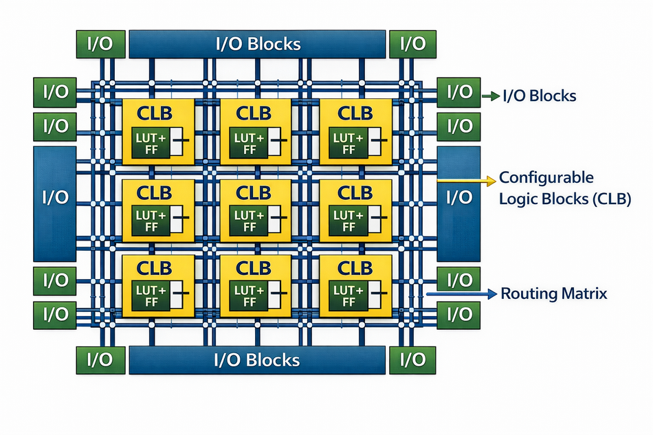
At the core of every FPGA is a two-dimensional array of configurable logic blocks (CLBs) interconnected by programmable routing and surrounded by I/O blocks. This basic architecture includes three elements:
Configurable logic blocks (CLBs): Each CLB contains multiple slices composed of lookup tables (LUTs), multiplexers, and flip‑flops that implement combinational and sequential logic. For example, the Xilinx Virtex-5 architecture uses 6-input LUTs, flip-flops, and multiplexers within each slice. Internally, these blocks implement digital logic gates using lookup tables (LUTs) and flip-flops. Modern devices also integrate block RAM, DSP slices, and high-speed transceivers to support high-bandwidth data flow and advanced digital signal processing workloads.
Interconnect network: Programmable interconnect wires and switch matrices route signals between CLBs and other resources, forming a mesh capable of arbitrary connections.
- I/O blocks (IOBs): IOBs provide the electrical interface to external pins. They include programmable input and output buffers and support different voltage levels.
In AMD/Xilinx 7‑series devices, each CLB contains two slices (SLICEL and SLICEM). A SLICEL houses four 6‑input LUTs and eight flip‑flops; a SLICEM can also implement distributed RAM or shift registers. Lookup tables implement arbitrary Boolean functions by storing truth table values in memory. Flip‑flops provide synchronous storage, and dedicated carry chains enable efficient arithmetic operations.
Intel’s FPGAs use adaptive logic modules (ALMs) instead of slices. An ALM includes LUTs, multiplexers, and an optional output register, supporting functions like adders and comparators. These ALMs, along with specialized blocks, form the programmable fabric.
Routing Architecture and Channel Organization
The routing network of an FPGA can occupy 80–90 percent of the total silicon area. In the commonly used island-style architecture, CLBs are placed at the intersections of horizontal and vertical routing channels.
FPGA routing is programmable, providing flexibility at the cost of variability in timing and power consumption. Delays introduced by routing often dominate overall signal propagation times, especially for long paths spanning multiple logic blocks. Similarly, power consumption is heavily influenced by routing capacitance and switching activity, making efficient routing essential for high-performance and low-power designs.
Types of Routing Resources
FPGA routing resources are hierarchically organized to provide both local flexibility and long-distance connectivity:
Local Routing:
These short wires connect logic elements within a single CLB or neighboring blocks. They provide low-latency connections ideal for combinational and sequential logic paths.
Short and Long Interconnect Lines:
Short interconnects handle connections between nearby CLBs.
Long or global interconnects span multiple rows or columns of CLBs, reducing the number of intermediate buffers but increasing wire capacitance. Designers must balance flexibility and timing when mapping critical signals to these lines.
Switch Matrices:
Switch matrices allow routing wires of different lengths and orientations to interconnect. They serve as programmable junctions that enable signals to traverse the FPGA fabric flexibly.
Connection Boxes:
Connection boxes link CLB inputs and outputs to available routing lines. Their design defines which wires each logic block can drive or sample, and their connectivity parameters influence placement and congestion.
Routing Channels:
Horizontal and vertical routing tracks, called channels, carry all wires connecting logic blocks. The number of tracks per channel, known as channel width, determines the maximum connectivity and directly impacts routing congestion.
Programmable Switches
Programmable switches are the fundamental building blocks of FPGA routing. They determine how logic blocks are connected to routing wires:
Multiplexers: Multiplexers select one of multiple input wires to connect to an output, providing flexible signal routing.
Pass Transistors: Simple on/off switches that connect two wire segments when enabled.
Configuration Control: Each switch is controlled by configuration memory (SRAM, flash, or antifuse). The combination of active switches defines the FPGA’s functional interconnect.
Switch design affects timing, area, and power. Poorly sized switches can introduce excessive delay or capacitance, limiting performance on critical paths. Modern FPGAs often combine different types of switches to optimize the tradeoff between flexibility and speed.
Routing Congestion and Design Challenges
Routing presents several challenges:
Timing Closure: Excessive path lengths or overused routing resources can result in violations of clock constraints.
Congestion: Concentrating high-demand logic in a small area forces detours for signals, resulting in increased delay and power consumption.
Tool Dependence: FPGA CAD tools perform automated placement and routing to optimize timing, congestion, and power. Engineers must provide constraints and floorplanning guidance to avoid bottlenecks.
Understanding the types of routing resources and programmable switches allows designers to anticipate congestion, optimize critical paths, and achieve efficient timing closure.
Input/Output Blocks (IOBs) and I/O Architecture
Role of I/O Blocks
Input/Output Blocks (IOBs) serve as the interface between the FPGA core and the external environment, enabling communication with sensors, memory devices, peripheral ICs, and other digital systems. They perform crucial functions such as buffering, level shifting, and signal conditioning, ensuring that internal FPGA signals can safely and reliably interact with external voltages and logic levels.
IOBs also play a critical role in timing closure, as signal propagation delays, drive strength, and input/output skew directly affect overall system performance. Correct I/O Configuration is also essential for effective debugging, as improper termination, voltage mismatch, or bank assignment can mimic logic errors within the FPGA core circuitry.
Many modern FPGAs provide programmable options for input and output behavior, including drive strength, slew rate, and termination control, allowing designers to optimize signal integrity and reduce electromagnetic interference (EMI).
Supported I/O Standards
FPGA IOBs support a wide variety of single-ended and differential I/O standards, enabling compatibility with a broad range of devices and interfaces:
Single-ended standards: These include LVCMOS and LVTTL, which are widely used for general-purpose logic signaling. Single-ended I/Os are typically simple to implement but may face limitations in high-speed or noisy environments.
Differential standards: Standards such as LVDS and SSTL improve noise immunity and signal integrity, especially at higher frequencies. Differential pairs carry complementary signals, reducing common-mode noise and enabling reliable high-speed communication.
High-speed serial interfaces: Many IOBs support multi-gigabit transceivers and high-speed serial protocols like PCIe, Ethernet, and Serial RapidIO. These interfaces rely on specialized IOB logic and dedicated clocking resources to achieve low-latency, high-throughput communication.
I/O Banks and Voltage Domains
FPGA IOBs are grouped into banks, each of which can operate at a distinct voltage domain. This organization allows the FPGA to interface with multiple external systems using different voltage levels simultaneously.
I/O banks provide isolation between voltage domains, ensuring that signals in one bank do not adversely affect neighboring banks. All IOBs within a bank must share compatible voltage standards. Designers must carefully assign signals to appropriate banks to avoid voltage conflicts, which could damage the device or lead to unreliable operation.
Dedicated Hardware Blocks in Modern FPGAs
Modern FPGAs integrate dedicated hardware blocks alongside configurable logic to accelerate data-intensive workloads, simplify design, and reduce reliance on general-purpose logic.
Block RAM (BRAM)
BRAM consists of dedicated memory blocks embedded within the FPGA fabric, often 36 Kb per block. BRAMs typically support true dual-port operation, enabling two independent reads or writes simultaneously, which is critical for high-throughput pipelines. They can be cascaded to form larger memories for FIFOs, buffers, or caches.
BRAMs are essential for storing intermediate results in digital signal processing, implementing line buffers in image and video processing, or serving as local memory for embedded processors. While versatile, BRAM has finite capacity, so designers must carefully balance its usage with logic and routing resources.
DSP Blocks
DSP blocks are specialized arithmetic units optimized for multiply-accumulate (MAC) operations. They support fixed-point and floating-point computation, making them ideal for digital filters, FFTs, AI inference kernels, and other signal processing workloads.
Modern FPGAs provide variable-precision DSP blocks, allowing designers to choose word lengths that optimize resource usage and performance. By offloading arithmetic-intensive operations to DSP slices, designers can significantly reduce logic utilization and achieve lower latency and power consumption compared with implementing MAC operations in LUTs and flip-flops.
Clock Management Tiles
Clock management is a critical aspect of FPGA design.
Clock management tiles (CMTs) include PLLs (phase-locked loops) and MMCMs (mixed-mode clock managers) that provide flexible clock generation, multiplication, division, and phase adjustment. These tiles enable designers to distribute multiple clock domains efficiently across the FPGA fabric and handle clock domain crossings safely.
Proper use of CMTs ensures synchronized operation of different blocks, reduces clock skew, and improves timing closure for high-performance designs.
Hard IP Blocks
Many modern FPGAs integrate hard IP blocks, which are pre-designed, optimized hardware cores for common interfaces and protocols. Examples include PCIe controllers, Ethernet MACs, DDR memory controllers, and transceivers. The advantages of hardened logic include predictable performance, lower power consumption, and reduced logic utilization, compared with implementing these functions in configurable fabric.
Hard IP blocks are essential for high-speed communication, memory interfacing, and standard protocol compliance, enabling designers to focus on application-specific logic rather than reinventing foundational components.
Configuration Technology and Programming Models
Configuration Memory Types
FPGA configuration memory can be implemented using several technologies:
SRAM-based FPGAs: Most modern FPGAs use volatile SRAM cells to store the configuration. This allows unlimited reprogramming and flexibility but requires loading the bitstream from external non-volatile memory at every power-up.
Flash-based FPGAs: Flash memory stores the bitstream non-volatilely, enabling instant-on behavior without external memory. Flash FPGAs offer robust operation and can be reprogrammed multiple times, though typically with fewer reprogramming cycles than SRAM.
Antifuse-based FPGAs: Antifuse technology creates permanent connections during programming, resulting in a one-time programmable device. Antifuse FPGAs provide high security and radiation tolerance, but cannot be reconfigured once programmed.
Configuration Methods
There are several standard methods to program an FPGA:
JTAG (Joint Test Action Group): A serial interface primarily used for testing and configuration in development and production environments.
SPI Flash / Parallel Flash: External non-volatile memory stores the bitstream, which the FPGA reads during power-up to configure itself.
Processor-Assisted Configuration: Embedded processors or microcontrollers load and manage the FPGA configuration, often enabling dynamic reconfiguration or partial updates during operation.
Volatility, Security, and Reliability
Configuration memory characteristics affect FPGA behavior and system reliability:
Power-Up Behavior: Volatile FPGAs require bitstream loading at every power cycle, while non-volatile FPGAs retain their configuration.
Bitstream Encryption: Modern devices support encryption to protect intellectual property and prevent unauthorized copying or tampering.
Radiation and Soft Errors: SRAM-based FPGAs are susceptible to single-event upsets in high-radiation environments. Error detection and correction mechanisms, as well as radiation-hardened variants, improve reliability in aerospace or nuclear applications.
Types of FPGAs
FPGAs can be classified based on application, capacity, and integration, ranging from low-cost devices for simple applications to high-performance platforms for demanding workloads.
High-End FPGAs
High-end FPGAs offer maximum logic density, performance, and advanced features, often using the latest process nodes (7 nm or below). These devices are suitable for data centers, advanced communications, and AI acceleration. Examples include Xilinx Virtex UltraScale+, AMD Versal Gen 2, and Intel Stratix 10/Agilex 5 families.
Mid-Range FPGAs
Mid-range FPGAs balance cost, performance, and resource availability. They are commonly used in industrial, automotive, and embedded applications where moderate performance is sufficient. Examples include Xilinx Kintex‑7 and Artix‑7, Intel Arria, and Lattice ECP3/ECP5 devices.
Low-End FPGAs
Low-end FPGAs prioritize low cost and power consumption, making them ideal for IoT, consumer electronics, and simple control applications. Examples include Lattice iCE40, Microchip PolarFire, and Xilinx Spartan series.
Specialized and Embedded FPGAs
As system complexity grows, vendors offer embedded FPGAs (eFPGAs) and other specialized FPGA variants. eFPGAs are IP blocks integrated into ASICs or SoCs, providing configurable logic, memory, and DSP blocks without requiring a separate FPGA package. They allow designers to tailor logic capacity, I/O, and aspect ratio, and can be reprogrammed after chip manufacture to reduce the need for expensive respins.
Compared with traditional discrete FPGAs, embedded FPGAs rely on on-chip interconnect and customizable resources rather than fixed external interfaces, enabling greater flexibility for specialized applications.
Traditional FPGA Design Flow
Hardware Description Languages and Simulation
Developing an FPGA design begins with design entry using hardware description languages such as VHDL, Verilog, or SystemVerilog. Engineers describe the desired behavior at the RTL level.
Simulation is used to verify functional correctness before synthesis.
Synthesis, Placement, and Routing
During synthesis, the HDL code is translated into a netlist of logical elements (LUTs, flip‑flops, DSP blocks).
Next, placement maps these logical elements onto specific configurable logic blocks (CLBs), and routing connects them through the FPGA’s programmable interconnect network. The goal is to minimize critical path delay while efficiently using available resources. Proper placement and routing are essential for achieving high performance, low power, and timing closure.
Bitstream Generation and Programming
After place‑and‑route, the tools generate a configuration bitstream. This binary file encodes the state of each programmable element and routing switch. Engineers load the bitstream into the FPGA using a programming cable or configuration interface (JTAG, SPI, or PCIe).
Recommended Reading: FPGA Programming: Theory, Workflow, and Practical Implementations
Debugging and In-System Verification
Debugging FPGA-based systems differs fundamentally from software debugging. Engineers rely on simulation, waveform analysis, and in-system logic analyzers to observe internal signals. Most FPGA vendors provide embedded debugging tools—such as Integrated Logic Analyzers (ILAs) and virtual probes—that allow real-time inspection of internal circuitry while the design is running on hardware.
High-Level Synthesis and Modern Design Tools
To reduce development time and abstract complexity, High-Level Synthesis (HLS) tools compile higher-level languages such as C/C++, OpenCL, or MATLAB into RTL. HLS enables algorithm developers to target FPGAs without deep HDL expertise while automatically generating pipeline registers, managing memory interfaces, and supporting parameterized designs. Popular tools include Xilinx Vitis/Vivado HLS, Intel HLS Compiler, and Mentor Catapult.
Modern workflows also integrate verification and testing frameworks such as Cocotb, Verilator, and GHDL, allowing advanced simulation and automated regression testing. CI/CD pipelines using Jenkins or GitLab streamline synthesis, simulation, and testing, improving collaboration and design quality.
Functional and domain-specific languages like Chisel, Bluespec SystemVerilog, and MyHDL provide additional abstraction, generating HDL code automatically. OpenCL and SYCL frameworks enable data-parallel programming across CPUs, GPUs, and FPGAs. With these tools, a single code base can target heterogeneous accelerators while leveraging FPGA fabric for low-latency, high-throughput execution, supporting domain-specific accelerators and emerging oneAPI/SYCL flows.
Advanced FPGA Architectures and Adaptive SoCs
Adaptive SoCs and Heterogeneous Integration
Recent FPGA families integrate heterogeneous components to create adaptive SoCs. The Intel Agilex 5 E‑Series, AMD Versal Gen 2, and Lattice Nexus 2 illustrate different philosophies:
Intel Agilex 5: The Agilex 5 FPGA and SoC portfolio is built on the Hyperflex® core architecture with distributed Hyper‑Registers to improve timing closure and performance compared with previous generations. Agilex 5 SoC devices integrate embedded processors such as dual Arm Cortex‑A76 and Cortex‑A55 cores alongside FPGA logic and hardened IP for high‑speed I/O and memory interfaces, enabling mixed hardware‑software systems on a single die.
AMD Versal Gen 2 Adaptive SoCs: AMD’s Versal Gen 2 family extends adaptive SoC integration with programmable logic, AI Engines, DSP engines, network‑on‑chip (NoC) fabrics, and hardened interfaces. Certain Versal Gen 2 devices support PCIe® Gen6 and CXL® 3.1 connectivity, offering very high host and accelerator interconnect bandwidth for data‑intensive compute applications. The programmable NoC provides an optimized interconnect between compute engines and integrated IP blocks, supporting multi‑terabit data paths with quality‑of‑service control.
These adaptive SoCs integrate hardened processors, AI accelerators, security blocks, and high‑speed interfaces, reducing board complexity and enabling end‑to‑end compute on a single chip.
Embedded FPGA IP and Chiplets
Embedded FPGA (eFPGA) IP allows designers to embed programmable logic directly within ASICs and SoCs. RF Wireless World explains that eFPGAs provide customizable LUT count, memory, and DSP resources and allow the designer to choose the foundry and I/O count. Because the logic fabric is inside the host chip, designers avoid external interfaces like PCIe, leading to lower latency and power. eFPGAs can be licensed from vendors and integrated into custom SoCs, enabling post‑manufacture updates and features such as in‑field upgradeability and hardware obfuscation.
High‑Bandwidth Memory and NoC
High‑end FPGAs integrate high‑bandwidth memory (HBM) stacks adjacent to the logic fabric. AMD’s Virtex UltraScale+ HBM devices embed up to 16 GB of HBM2, delivering around 460 GB/s, while Intel Agilex devices provide hardened memory network‑on‑chip (NoC) interfaces to support multi‑terabyte per second bandwidths ( as per vendor documentation). The Microchip comparison notes that Versal Gen 2 features optional HBM and next‑generation transceivers for extreme bandwidth, whereas Agilex 5 and Versal provide DDR5/LPDDR5X support. On‑chip HBM reduces memory latency and energy per bit, enabling data‑intensive applications like AI inference, database acceleration, and scientific computing.
Network‑on‑Chip and 3D Integration
To support large designs and high connectivity, modern FPGAs employ network‑on‑chip (NoC) fabrics that route data between logic clusters, memory, and I/O. Stratix 10 and Agilex families implement multi‑plane NoCs with quality‑of‑service and protocol handling. Some devices also use 3‑D chip stacking and heterogeneous chiplets. For example, Intel’s 3D SiP technology integrates transceiver tiles with the core FPGA fabric, optimizing high‑speed I/O.
Partial and Dynamic Reconfiguration
Partial reconfiguration (PR) allows a portion of the FPGA to be reprogrammed while the rest of the device continues running. When this reprogramming happens at runtime without stopping the system, it is referred to as dynamic reconfiguration. This capability enables FPGAs to adapt to changing workloads on the fly, optimize hardware usage, and minimize downtime.
Key benefits of dynamic partial reconfiguration include:
Resource Optimization: Hardware blocks used at different times—such as FFT engines versus FIR filters—can share the same FPGA area, reducing wasted logic resources.
Power Savings: Only the reconfigurable logic that is actively needed is powered and loaded, which lowers dynamic power consumption.
Smaller Bitstreams and Faster Updates: Because only the reconfigurable region is updated, dynamic updates require transferring smaller bitstreams, enabling fast runtime switching.
System Adaptability: Dynamic PR enables real-time changes in applications such as software-defined radios, adaptive AI accelerators, or multi-protocol communications systems. For example, a radio can switch between LTE and 5G modes without halting the rest of the system.
Recommended Reading: ASIC vs FPGA: A Comprehensive Comparison
FPGAs Vs CPUs Vs GPUs
The table compares CPU, GPU, and FPGAs.
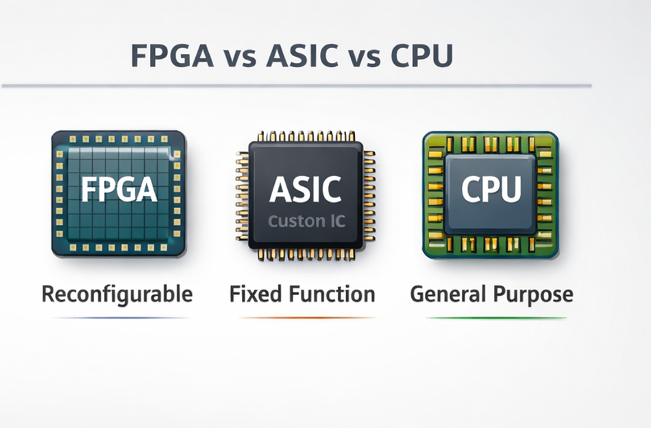
Characteristic | CPU | ASIC | FPGA |
Core Functionality | General‑purpose; sequential tasks | Fixed-function hardware; custom logic | Customizable logic; parallel pipelines |
Flexibility | Moderate – software programmable but fixed hardware | Very low – fixed functionality once fabricated | Highly reconfigurable for specific tasks |
Performance | Good across many tasks | Very high for targeted tasks; highly optimized | Optimizable to outperform CPUs/GPUs for targeted tasks |
Efficiency | Moderate energy efficiency | Very high; optimized for task | Low power due to customized circuits |
Latency | Higher latency | Nanosecond-scale; hardware-level execution | Microsecond‑scale latency; dedicated data paths |
Future Directions and Market Outlook
Market Growth and Key Drivers
The global FPGA market is projected to grow at a compound annual growth rate exceeding 10 percent through 2032, driven primarily by expanding demand in artificial intelligence, edge computing, 5G infrastructure, and the Internet of Things. Market analyses indicate that mid-range FPGAs currently account for the largest share of revenue, reflecting their balance of cost, performance, and power efficiency across industrial and embedded applications.
At the same time, high-end FPGAs represent the fastest-growing segment, fueled by requirements in high-bandwidth communications, aerospace and defense systems, and data-center acceleration, where extreme throughput, low latency, and integration of advanced memory and interfaces are critical.
Emerging Architectures and Technology Trends
Several architectural and ecosystem trends are shaping the future evolution of FPGAs:
Adaptive SoCs with Integrated AI Engines:
FPGA platforms are increasingly incorporating dedicated AI tensor cores and neural processing engines, as seen in adaptive SoC families such as AMD Versal Gen 2. These tightly coupled accelerators enable efficient execution of machine learning and deep learning workloads alongside programmable logic, reducing latency and improving energy efficiency.High-Bandwidth Memory and Chiplet-Based Integration:
The adoption of on-package high-bandwidth memory (HBM) and memory-centric network-on-chip architectures is expected to expand, allowing FPGAs to support data-intensive workloads such as AI inference, analytics, and high-performance computing. Chiplet-based designs will further enable vendors to mix process nodes, optimize I/O, and scale device capability without monolithic die complexity.Embedded FPGA (eFPGA) IP and Heterogeneous Systems:
The use of eFPGA IP blocks within ASICs and SoCs is expected to grow as designers seek post-fabrication flexibility, enhanced security, and protection against hardware obsolescence. eFPGAs enable late-stage feature updates, hardware obfuscation, and workload-specific customization within otherwise fixed silicon.AI-Driven and Dynamic Partial Reconfiguration:
Future FPGA systems are expected to leverage intelligent runtime management, dynamically loading and unloading hardware modules based on workload demands, power budgets, and thermal constraints. This approach combines partial reconfiguration with AI-based scheduling to maximize utilization and system efficiency.High-Level Programming and Open Tool Ecosystems:
Continued advances in high-level synthesis, functional hardware description languages, and open programming frameworks such as oneAPI, SYCL, and OpenCL are lowering the barrier to FPGA adoption. When combined with modern verification tools and CI/CD workflows, these ecosystems are helping democratize hardware acceleration and integrate FPGAs more naturally into software-centric development environments.
In summary, the future of FPGAs lies in deeper system integration, adaptive computing, and improved programmability. As architectures evolve beyond standalone programmable logic into heterogeneous, software-defined platforms, FPGAs are positioned to remain a key technology across edge, cloud, and embedded computing domains.
Conclusion
FPGAs occupy a distinct position in the hardware landscape, offering customizable logic that bridges the gap between ASICs and general‑purpose processors. Their architecture—built from configurable logic blocks, programmable routing, and specialized resources such as memory, DSPs, and transceivers—provides unparalleled flexibility.
Effective FPGA design requires a solid understanding of both architectural fundamentals and practical design workflows. In practice, FPGAs are widely used for hardware prototyping, allowing engineers to validate architectures, test algorithms, and evaluate performance before committing to ASIC fabrication.
As demand grows across AI acceleration, edge computing, 5G infrastructure, and IoT, FPGAs are evolving beyond standalone programmable logic into highly integrated, software-defined computing platforms. Adaptive SoCs, embedded FPGA IP, and intelligent runtime reconfiguration will continue to shape the next generation of hardware systems, ensuring that programmable logic remains a critical enabler of performance, flexibility, and innovation in modern computing.
Frequently Asked Questions (FAQ)
What are configurable logic blocks (CLBs)?
CLBs are the fundamental units of an FPGA. Each CLB contains slices made of look‑up tables (LUTs), flip‑flops, and multiplexers. LUTs implement combinational logic, while flip‑flops store sequential state. In Xilinx devices, each CLB contains multiple slices with four 6‑input LUTs and eight flip‑flops. Intel uses adaptive logic modules (ALMs) with similar functionality.
How does FPGA routing work?
FPGAs use a mesh of programmable interconnect wires and switch boxes to connect CLBs. Routing channels of various lengths, along with connection boxes that link CLB pins to wires, allow flexible signal paths. The routing network can occupy most of the silicon area, and its configuration is determined during place‑and‑route.
What is partial reconfiguration?
Partial reconfiguration is the ability to modify a portion of the FPGA while the rest of the device continues running. It enables resource sharing, power savings, and adaptability. Designers partition the device into static and reconfigurable regions and create partial bitstreams that can be loaded on demand.
What are the differences between FPGA and eFPGA?
Traditional FPGAs are standalone chips with fixed amounts of LUTs, memory, and DSP blocks, and external interfaces like PCIe or SERDES. eFPGAs are IP blocks integrated into ASICs or SoCs, allowing designers to specify the amount of programmable logic, memory, and DSPs and choose the foundry. eFPGAs provide on‑chip interconnect, lower latency, and customization after manufacturing.
How do FPGAs compare to GPUs for AI inference?
FPGAs can be tailored to the specific compute and memory requirements of AI inference, achieving microsecond latencies and operating at power levels around 10 W, whereas GPUs typically require 75 W or more. FPGAs support parallel pipelines and customizable precision, enabling high throughput and energy efficiency for inference workloads. GPUs, however, are easier to program and excel at training deep networks.
Which FPGA families are most relevant in 2025?
Intel’s Agilex 5 E‑Series, AMD’s Versal Gen 2, and Lattice’s Nexus 2 illustrate current trends: integrating AI engines, Arm processors, high‑bandwidth memory, and advanced transceivers. These platforms target edge computing, data‑center AI, 5G, and IoT applications.
What tools can simplify FPGA development?
High‑level synthesis tools (e.g., Xilinx Vitis/Vivado HLS, Intel HLS Compiler) compile C/C++ or OpenCL into RTL, reducing development effort. Modern IDEs, simulation frameworks, and CI/CD pipelines further streamline design, verification, and deployment.
References
[1] Fortune Business Insights, “Field Programmable Gate Array (FPGA) Market Size, Share and Industry Analysis,” Fortune Business Insights, 2024. [Online]. Available: fortunebusinessinsights.com
[2] eeNews Europe, “FPGA Market Forecast,” eeNews Europe, 2023. [Online]. Available: eenewseurope.com
[3] Digilent Inc., “Understanding the 7-Series FPGA Configurable Logic Block,” Digilent Technical Resources, 2022. [Online]. Available: digilent.com
[4] Digilent Inc., “FPGA Building Blocks: BRAM, DSP, and I/O,” Digilent Technical Resources, 2022. [Online]. Available: digilent.com
[5] K. Compton and S. Hauck, “Reconfigurable Computing: A Survey of Systems and Software,” ACM Computing Surveys, vol. 34, no. 2, pp. 171–210, 2002. (Referenced via island-style routing overview)
[6] Intel Corporation, “Adaptive Logic Modules (ALMs) Architecture Overview,” Intel Documentation, 2023. [Online]. Available: intel.com
[7] Intel Corporation, “DSP Architecture Features and Benefits in Intel FPGAs,” Intel White Paper, 2023. [Online]. Available: intel.com
[8] RF Wireless World, “FPGA Architecture and Basic Building Blocks,” RF Wireless World, 2021. [Online]. Available: rfwireless-world.com
[9] RF Wireless World, “FPGA vs eFPGA: Key Differences,” RF Wireless World, 2021. [Online]. Available: rfwireless-world.com
[10] Fidus Systems, “The Role of FPGAs in AI Acceleration,” Fidus Systems Blog, 2024. [Online]. Available: fidus.com
in this article
1. Key Takeaways2. Introduction3. Fundamentals of FPGA Architecture4. Core Architectural Elements of an FPGA5. Routing Architecture and Channel Organization6. Input/Output Blocks (IOBs) and I/O Architecture7. Dedicated Hardware Blocks in Modern FPGAs8. Configuration Technology and Programming Models9. Types of FPGAs10. Traditional FPGA Design Flow 11. High-Level Synthesis and Modern Design Tools12. Advanced FPGA Architectures and Adaptive SoCs13. Partial and Dynamic Reconfiguration14. FPGAs Vs CPUs Vs GPUs 15. Future Directions and Market Outlook16. Conclusion17. Frequently Asked Questions (FAQ)18. References