NMOS Symbol: Comprehensive Guide to N Channel MOSFET Symbols, Operation and Applications
A technical deep dive into the NMOS symbol, working, and device behavior, contribution in analog design and advanced NMOS technologies in the modern age.

16 Oct, 2025. 11 minutes read
Key Takeaways
The NMOS symbol shows an n-channel MOSFET, a voltage-controlled device using electrons as carriers. Its arrow points inward, showing current from the p-type substrate to the n-channel.
Symbol variations indicate device type: a solid line is depletion-mode (normally-on), a dashed line is enhancement-mode (normally-off).
NMOS switches on when the gate-to-source voltage exceeds the threshold. Enhancement-mode forms a channel only if VGS>Vth, creating cut-off, linear, and saturation regions.
Key analog parameters are small-signal transconductance (gm), output resistance (ro), and intrinsic gain (Av)
Modern NMOS evolved from planar to FinFET and Gate-All-Around (GAA) structures for better short-channel control. Strained silicon boosts electron mobility by ~70%, increasing speed; GAA appeared at the 3-nm node.
Introduction
The metal‑oxide‑semiconductor field‑effect transistor (MOSFET) revolutionized electronics by enabling large‑scale integration with low power consumption and high input impedance. Among its variants, the n‑channel MOSFET (NMOS) is the workhorse of digital and analog circuits because electrons have higher mobility than holes, allowing faster switching. Understanding the NMOS symbol is essential for circuit designers: the symbol conveys not only the device type but also its operating mode. This article offers a comprehensive exploration of the NMOS symbol and dives into the physics, small‑signal parameters, and practical implementations of NMOS transistors. We target digital design engineers, hardware engineers, and electronics students seeking an authoritative reference on n‑channel MOSFETs.
Suggested Reading: JFET vs MOSFET: A Comprehensive Engineering Analysis and Selection Guide
Fundamentals of MOSFETs and N‑channel devices
MOSFET Construction and Charge Carriers
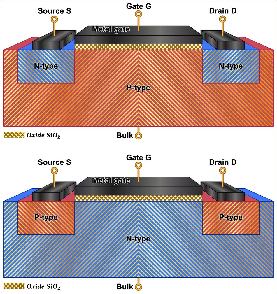
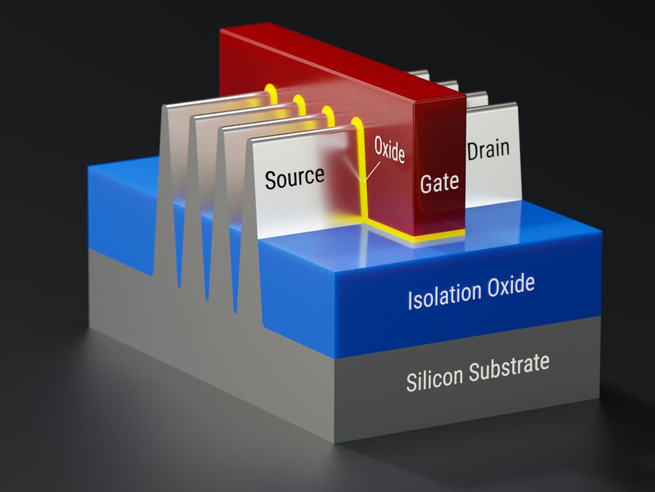
A MOSFET consists of four terminals: gate (G), source (S), drain (D), and body or substrate (B). In an NMOS transistor, the source and drain regions are heavily n‑type doped while the body is p‑type. A thin insulating layer of silicon dioxide isolates the gate from the channel.
When a positive gate voltage is applied, it attracts electrons to the p‑type surface, inverting it to form an n‑type channel between the source and drain. Because the gate is insulated, no steady‑state current flows into the gate; the device is voltage‑controlled and exhibits extremely high input resistance.
An NMOS device conducts current via electrons, which have roughly three times the mobility of holes in typical silicon. This higher mobility translates to lower on‑resistance and faster switching than p‑channel MOSFETs.
Conversely, a P‑channel MOSFET uses P‑type doped source and drain in an n‑type body; its arrow points outwards, and it turns on when the gate is pulled negative relative to the source.
Complementary MOS (CMOS) circuits pair NMOS and PMOS transistors to achieve low static power consumption and full‑swing output levels.
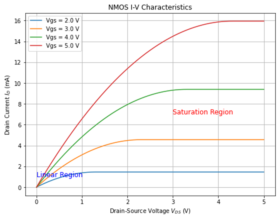
Regions of Operation
The drain current (Id) of an NMOS transistor depends on the gate‑to‑source voltage (Vgs) and drain‑to‑source voltage (Vds). Three operating regions are identified:
Cut‑off: When Vgs ≤ Vth_th (the threshold voltage), no inversion channel is formed and Id ≈ 0.
Linear/ohmic (triode): When Vgs > Vth and Vds < (Vgs – Vth), the transistor behaves like a voltage‑controlled resistor. The current rises roughly linearly with Vds. Designers often exploit this region for analog switches and variable resistors.
Saturation: When Vgs > Vth and Vds ≥ (Vgs – Vth), the channel becomes pinched off near the drain, and Id is nearly independent of Vds. Saturation is the preferred region for amplifiers because the drain current is controlled primarily by Vgs.
The threshold voltage Vth itself is influenced by the body effect: if the body voltage differs from the source, the threshold increases according to the body effect coefficient γ and surface potential. NMOS devices are often connected with the body tied to the source to eliminate this effect and to avoid forward biasing the substrate diode.
Further Reading: How Do MOSFETs Work: Comprehensive Technical Guide for Engineers (2025)
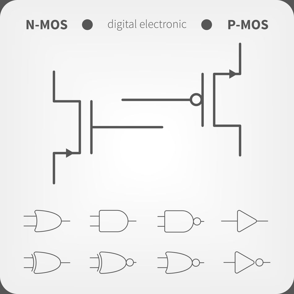
NMOS Symbol and its Variations
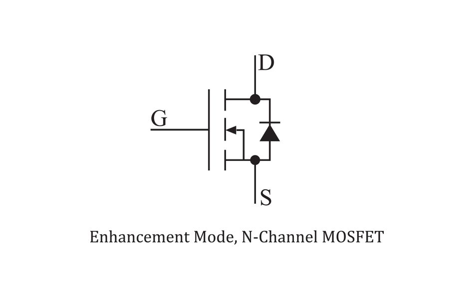
The standard NMOS symbol is a concise graphical representation of the device. The three external terminals—gate, drain, and source—are drawn as lines emerging from a channel. A fourth terminal (body) may be shown connected to the substrate or to the source. Several important details are encoded:
Arrow direction: An arrow on the body connection indicates the direction of conventional current flow between the substrate and the channel. For NMOS transistors, the arrow points toward the channel or “in”, a mnemonic captured by “n is in”. By contrast, in p‑channel devices, the arrow points outwards.
Channel line style: A solid channel line denotes a depletion‑mode (normally‑on) MOSFET, whereas a dashed or broken line denotes an enhancement‑mode (normally‑off) device. Enhancement‑mode devices require Vgs > Vth to conduct; depletion‑mode devices conduct even at zero gate voltage.
Terminal location: The gate electrode is drawn adjacent to the channel. The source and drain are typically interchangeable in long‑channel MOSFETs. However, short‑channel devices have an asymmetric structure; designers often label the source as the terminal with the lowest voltage.
Body connection: In integrated circuits, the body is usually tied to the lowest potential (ground for NMOS). In 3‑terminal representations, the body is implicitly connected to the source; in 4‑terminal symbols, the body arrow clarifies the device type.
Different schematic styles exist. In digital logic diagrams, the bulk connection may be omitted, and the arrow may be placed on the source or drain to indicate type.
In analog integrated circuit schematics, the body connection is drawn explicitly to model the body effect and to allow biasing networks. Depletion‑mode NMOS transistors are sometimes used as load devices in NMOS logic; these devices are depicted with a solid channel line.
Recommended Reading: High-Performance MOSFETs Driving Excellence and Innovations in Automotive Electronics
NMOS Device Physics and Large‑signal Equations
Formation of the Inversion Channel
When Vgs exceeds Vth, electrons accumulate near the gate oxide, forming an n‑type inversion channel. The channel allows current to flow from drain to source when a voltage Vds is applied. In an n‑channel MOSFET, the drain is usually at a higher potential than the source, so electrons flow from source to drain, while current (conventional positive flow) flows from drain to source.
The threshold voltage arises from the need to balance charges in the oxide and substrate. Factors influencing Vth include doping concentration, oxide thickness, temperature and the source‑body voltage. The body effect modifies Vth according to:

where:
Vt0 is the threshold voltage at zero substrate bias,
γ is the body effect coefficient, which quantifies how the threshold voltage changes with substrate bias,
ψs is the surface potential (typically related to twice the Fermi potential),
VSB is the source-to-body (substrate) voltage.
Large‑Signal Drain Current
Using a simplified Shichman–Hodges model, the drain current in the linear and saturation regions can be expressed as:
Linear Ohmic Region (Vds < Vgs - Vth): In this region, the MOSFET behaves like a voltage-controlled resistor, and current increases approximately linearly with Vds. It is represented by the following equation:

- Saturation region (Vds ≥ Vgs−Vth): Here, the channel is pinched off near the drain, and the current saturates to a nearly constant value independent of Vds.

Here,
u is the carrier mobility
Cox is the oxide capacitance per unit area
W, L are the channel width and length
Channel‑length Modulation
In practice, the drain current is not perfectly flat in saturation because the effective channel shortens with increasing Vds. This channel‑length modulation is quantified by λ. Including λ, the saturation drain current becomes:

where λ has units of V⁻¹ and typical values around 0.02 for long‑channel devices. Channel‑length modulation reduces the output resistance, and finite drain conductance must be accounted for in analog design.
Depletion‑mode NMOS devices
While most NMOS transistors are enhancement‑mode, depletion‑mode NMOS devices exist. In a depletion‑mode transistor the channel is doped such that conduction occurs at zero gate bias; applying a negative gate voltage depletes carriers and turns the transistor off. In circuit diagrams these devices are shown with a solid channel line. Depletion NMOS transistors are used as load elements in NMOS logic and as current sources.
Suggested Reading: N-Channel MOSFET Basics: Theory, Operation and Practical Implementations
Small‑signal Modeling and Key Parameters
When analyzing amplifiers or RF circuits, we linearize the MOSFET around a bias point to obtain its small‑signal model. This model replaces the nonlinear characteristics with linear conductances and capacitances that approximate the device’s incremental response.
Transconductance (gm)
Transconductance represents the incremental change in drain current per unit change in gate‑source voltage. Small‑signal transconductance is linear and saturation region is given as:

These expressions show that gm is proportional to the device’s width‑to‑length ratio and to the overdrive voltage Vgs – Vth in saturation.
Output resistance (ro)
Finite output resistance arises from channel‑length modulation. The small‑signal output resistance in saturation is approximately the inverse of the channel‑length modulation current:

Because λ increases as the channel length is reduced, short‑channel devices have smaller ro and thus lower intrinsic gain. Analog designers often cascade devices or use cascode topologies to improve output resistance.
Intrinsic voltage gain (Av)
The maximum small‑signal voltage gain of a single NMOS transistor is the product of its transconductance and output resistance:

Modern CMOS processes yield intrinsic gains between 5 and 10, necessitating multistage amplifiers to achieve higher gains.
Body‑effect Transconductance (gmb)
When the body is not tied to the source, changes in body voltage influence the threshold voltage and thus the drain current. The body‑effect transconductance is defined as:

where η is the back‑gate transconductance parameter, typically between 0 and 3. In many circuits, the body is tied to the source, making gmb negligible.
Recommended Reading: Silicon Semiconductor: A Comprehensive Guide to Silicon and its Use in Semiconductor Technology
Practical NMOS devices and datasheet parameters
Commercial NMOS transistors range from tiny logic‑level MOSFETs used in microcontroller interfaces to large power MOSFETs capable of handling tens or hundreds of amperes.
Key datasheet parameters include maximum drain‑source voltage (Vds), continuous drain current (Id), threshold voltage (Vgs(th)), gate charge, drain‑source on‑resistance (Rds(on))) and input capacitance. The following table summarizes representative values for two popular small‑signal NMOS devices based on their datasheets:
Device | Vds_max (V) | Id_max (A) | Vgs(th) (V) | Rds(on)) (Ω) |
2N7000 | 60 | 0.2 | 0.8–3 | ~2.5–5 |
BSS138 | 50 | 0.22 | 0.8–1.5 | 3.5 (10 V), 6 (4.5 V) |
The 2N7000 and its surface‑mount variant 2N7002 are popular for driving relays and logic translation because of their low threshold (~2 V), low input capacitance (~22 pF) and fast switching (7 ns).
The BSS138 features a lower gate threshold (0.8–1.5 V) and thus can be driven directly from 3.3‑V logic; it is widely used in level shifters and I²C translation boards.
For higher current applications, power MOSFETs employ vertical structures with source and drain on opposite sides of the silicon wafer. Trench MOSFETs (for <200 V) use deep trenches to maximize channel width and minimize Rds(on), while planar MOSFETs (for higher voltages) rely on a thick epitaxial layer to support voltage.
The on‑resistance comprises contributions from source and drain diffusion resistance, channel resistance, accumulation resistance, epitaxial resistance and substrate resistance. Power MOSFET datasheets also specify gate charge and switching times to help size gate drivers.
Suggested Reading: Understanding the MOSFET Symbol: Theory and Practical Insights for Engineers
NMOS in Digital design
NMOS logic and its limitations
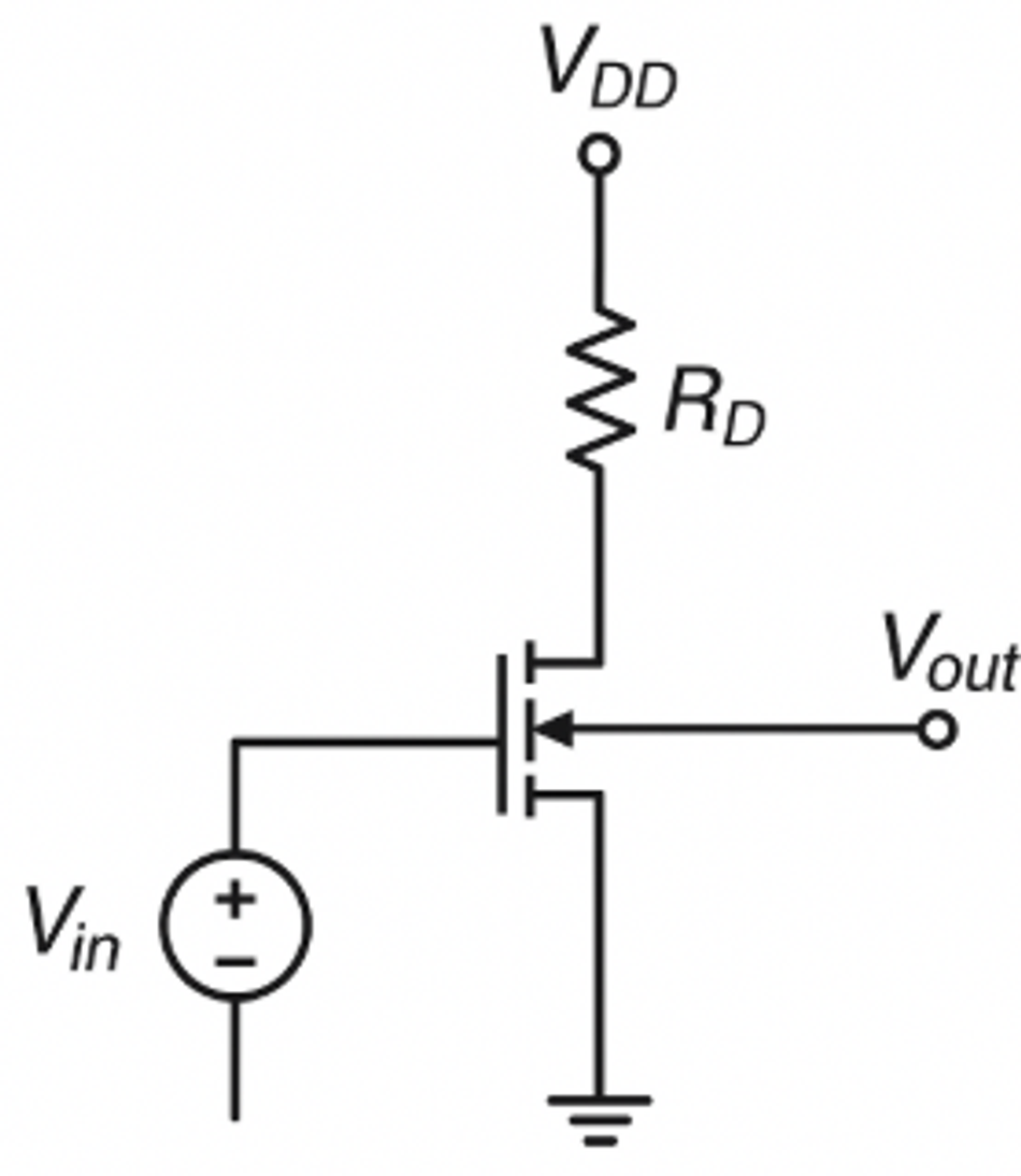
Before CMOS became the dominant technology, logic gates were built exclusively from NMOS transistors. An NMOS inverter consists of an NMOS transistor and a resistor load. When the input is high, the transistor conducts and pulls the output low; when the input is low, the transistor is off and the resistor pulls the output high.
NMOS logic was simple to fabricate and faster than PMOS but consumed static power because current flows continuously through the load when the output is low. To reduce static power, depletion-mode NMOS transistors were used as load devices, thereby eliminating the need for an external resistor and improving noise margins.
Despite its simplicity, NMOS logic suffers from several drawbacks. The high output (logic 1) is degraded because the load device conducts, causing a voltage drop. Noise margins are smaller than in CMOS, and the static current results in significant power dissipation and heat generation.
Consequently, CMOS logic—employing complementary NMOS and PMOS transistors in a push‑pull configuration—replaced NMOS logic in the 1980s and remains dominant today because it consumes negligible static power and offers full rail‑to‑rail swings.
Suggested Reading: PMOS vs NMOS: Unraveling the Differences in Transistor Technology
Transistors as digital switches and pull‑down devices
In modern digital circuits, NMOS transistors function primarily as pull‑down switches in CMOS gates. A NAND gate, for example, uses series NMOS devices to pull the output low only when all inputs are high, while parallel PMOS devices pull the output high.
Suggested Reading: Transistor as a Switch: Theory and Practical Implementation for Digital and Hardware Engineers
NMOS in analog design
Common‑source Amplifiers
The common‑source amplifier is the MOSFET analog of the BJT common‑emitter amplifier. A resistor or current source ro loads the drain, and the input signal is applied to the gate.
Differential pairs
NMOS transistors are the building blocks of differential amplifiers, where two transistors share a common current source. Differential pairs provide common‑mode rejection and form the input stage of operational amplifiers. The gain and linearity depend on the matching of the transistors and the ratio of gm to ro.
Advanced NMOS technologies and scaling trends
Strained silicon and mobility enhancement
To continue Moore’s law beyond the sub‑100 nm era, engineers have introduced techniques to enhance carrier mobility. One method is strained silicon, where a silicon channel is grown on a relaxed silicon–germanium (SiGe) substrate.
The lattice mismatch stretches the silicon lattice, increasing electron mobility by about 70 % and boosting switching speed by roughly 35 %. Strained silicon is widely used in modern NMOS transistors to achieve higher drive current without shrinking the channel length.
FinFETs
Planar NMOS transistors face severe short‑channel effects and leakage at gate lengths below 30 nm. FinFETs (fin‑field‑effect transistors) address this by employing a three‑dimensional structure: the channel forms in a thin vertical fin protruding from the substrate, and the gate wraps around the fin on three sides.
This architecture improves electrostatic control, allowing further scaling. FinFETs were introduced commercially at the 22‑nm technology node and remain the workhorse of advanced logic processes.
Gate‑all‑around (GAA) nanosheet FETs
The next evolution is the gate‑all‑around (GAA) FET, where the gate surrounds the channel on all four sides. GAA transistors use stacked horizontal nanosheets or nanowires to maximize channel width and reduce leakage. Samsung introduced 3‑nm GAA devices in 2022, and Intel and TSMC plan to adopt GAA around 2024–2026. GAA technology continues the trend of improving gate control while maintaining high drive current.
Conclusion
The NMOS symbol conveys device type, mode, and substrate connection. Understanding it is key to using n-channel MOSFETs effectively. We examined channel formation, large-signal behavior, and small-signal parameters critical for analog performance. Knowledge of channel-length modulation, body effect, parasitic capacitances, and transconductance is vital for optimizing digital and analog circuits.
Modern NMOS technology advances from planar to FinFET and gate-all-around nanosheets, enhanced by strained silicon. These innovations boost speed and reduce power but add modeling complexity. Mastering NMOS basics enables engineers to design robust microcontroller interfaces, switching regulators, and high-speed amplifiers efficiently.
Further Reading: Circuit Symbols: A Comprehensive Guide for Electronics Engineers
FAQs
What does the arrow in the NMOS symbol indicate?
The arrow on the body connection shows the direction of conventional current flow between the substrate and the channel. In an NMOS transistor the arrow points inward toward the channel (often remembered by the phrase “n is in”). In PMOS devices the arrow points outward.
How can I tell if a MOSFET is enhancement‑ or depletion‑mode from the symbol?
Examine the channel line in the symbol. A dashed channel line indicates an enhancement‑mode MOSFET, which is normally off and requires Vgs > Vth to conduct. A solid channel line indicates a depletion‑mode MOSFET, which conducts at zero gate bias and requires a negative gate voltage to turn off.
Why are NMOS transistors faster than PMOS transistors?
Electrons, the carriers in NMOS devices, have higher mobility than holes, the carriers in PMOS devices. This higher mobility results in lower on‑resistance and faster switching for NMOS transistors.
Why is the body often connected to the source in NMOS circuits?
Connecting the body (substrate) to the source ensures that the source‑body voltage is zero. This eliminates the body effect, which otherwise increases the threshold voltage and reduces transconductance. It also prevents the intrinsic body diode from becoming forward biased.
What is channel‑length modulation and how does it affect circuit design?
Channel‑length modulation occurs when increasing Vds shortens the effective channel length, causing the drain current in saturation to rise slightly with Vds. It is modeled by the parameter λ. A larger λ reduces the small‑signal output resistance r_o ≈ 1/(λ Id), limiting the voltage gain of amplifiers.
How do I choose an NMOS transistor for a particular application?
Consider the maximum drain‑source voltage (Vds), continuous drain current (Id), threshold voltage (Vgs(th)), gate charge and drain‑source on‑resistance (Rds(on))). For logic‑level switching, choose MOSFETs with low Vgs(th) (< 2 V) and low Rds(on)). Datasheets for devices like 2N7000 and BSS138 provide these parameters.
What are FinFETs and why are they important?
FinFETs are three‑dimensional MOSFETs where the channel forms in a vertical fin and the gate wraps around three sides. This geometry improves gate control and mitigates short‑channel effects. FinFETs were introduced at the 22‑nm technology node and have enabled continued scaling of CMOS technology.
References
“MOSFETs,” Electronics Tutorials. https://www.electronics-tutorials.ws/transistor/tran_6.html
“NMOS and PMOS,” AnySilicon. https://anysilicon.com/introduction-to-nmos-and-pmos-transistors
“MOSFET,” Wikipedia. https://en.wikipedia.org/wiki/MOSFET
“Threshold voltage,” Wikipedia. https://en.wikipedia.org/wiki/Threshold_voltage
“NMOS logic,” Wikipedia. https://en.wikipedia.org/wiki/NMOS_logic
“The Future of The Transistor,” SemiAnalysis. https://semianalysis.com/2023/02/21/the-future-of-the-transistor
“2N7000 MOSFET Datasheet,” Vishay. https://www.vishay.com/docs/70226/70226.pdf
“BSS138 MOSFET Datasheet,” Good-Ark Semi. https://goodarksemi.com/docs/datasheets/mosfets/BSS138.pdf
“MOSFET Construction and Operating Regions,” BYJU’s. https://byjus.com/physics/mosfet
“Small-Signal MOSFET Models,” All About Circuits. https://www.allaboutcircuits.com/technical-articles/small-signal-mosfet-models-for-analog-ic-design
in this article
1. Key Takeaways2. Introduction3. Fundamentals of MOSFETs and N‑channel devices4. NMOS Device Physics and Large‑signal Equations5. Small‑signal Modeling and Key Parameters6. Practical NMOS devices and datasheet parameters7. NMOS in Digital design8. NMOS in analog design9. Advanced NMOS technologies and scaling trends10. Conclusion11. FAQs12. References