Unfolding the Future: The Evolution and Impact of Printed Electronics
Printed electronics, characterized by their low cost and versatility through processes like inkjet or screen printing, are pivotal in advancing technologies such as wearable tech and the Internet of Things.

13 Mar, 2024. 7 minutes read
Behind the rise of many of today’s latest technologies, from wearable tech to the Internet of Things, are printed electronics. As we’ll explore throughout this article, these low-cost and highly versatile electronic devices, which can be made using existing printing processes like inkjet or screen printing, present a vast array of benefits and potential applications. We will also be taking a closer look at Canadian company Voltera and how its additive printing technology for electronics is unlocking greater accessibility and innovation for printed electronic development.
Understanding Printed Electronics
In general, the term printed electronics refers to all electronics that are manufactured by printing conductive and dielectric materials onto a substrate to create a circuit. This technique is not unlike two-dimensional printing on paper. In fact, many printed electronics are made using conventional printing techniques, like inkjet printing and screen printing. These technologies have been adapted to deposit inks embedded with conductive and dielectric materials, such as metals or carbon-based materials, onto rigid or flexible substrates, including paper, polymer films, and more.
This approach differs from conventional electronic production methods, such as physical vapor deposition (PVD) and etching, which are both used in the production of printed circuit boards (PCBs). The PVD process, for instance, is a type of vacuum deposition that applies fine films and coatings to a substrate.[1] In the etching process, conductive material (usually copper) is selectively removed from a printed circuit board to create an electronic circuit.[2] While these processes are both more established than printed electronics, they are more limited in terms of design and flexibility, typically requiring the use of a rigid substrate and an enclosure. They are also more costly, requiring a steep investment in specialist equipment.
Sustainability is another key consideration with conventional PCB production processes. PCB manufacturing is not only extremely energy intensive, it also generates hazardous waste, and consumes a significant amount of water (as much as “1.5m^3 for every m^2 of board processed”).[3] This translates to over one ton of water for every square meter of circuit board.
Printed electronics and the processes used to make them are ever-evolving. For example, advances in material science are opening up more types of printable materials, including conductive inks that are engineered to be stretched while retaining their properties. The ability to print flexible conductive elements onto stretchable substrates is owed to developments in the field of nanotechnology. Specifically, the ability to produce and embed nanoparticles made from conductive or dielectric materials optimized for stretch and flexibility into a printable ink.
Benefits of Printed Electronics
Printed electronics offer a number of advantages compared to more conventional electronics and create previously impossible opportunities. Among these benefits are design freedom, cost-effectiveness, and greater sustainability.
Design freedom
One of the main advantages of printed electronics is the ability to realize a greater range of designs. Using printing technologies it is possible to print electronics on a larger surface area, as well as to design thinner sensors that can be seamlessly embedded into products. This includes very thin devices printed on flexible substrates, which can conform to a product’s surface. Unlike in rigid PCB design, where the circuit determines the form factor of the product, printed flexible electronics can be adapted to a specific shape, opening up opportunities for device design, compactness, and conformability.
Cost effective
Printed electronics also have the benefit of being more affordable to produce than conventional electronics. This is due to a number of factors. First, the equipment required to print electronics is itself low cost compared to conventional PCB production methods. Second, it is possible to deposit conductive inks onto low-cost substrates, such as paper or plastic films, which are cheaper than PCB substrates, traditionally made from FR-4, a fiberglass and epoxy composite. Third, printed electronics are cost-effective even for small volumes, which makes the technology more accessible to small businesses and research labs with limited resources.
Sustainability
Another distinct advantage of printed electronics is that they can have a smaller environmental impact. For one, the printing process involved in depositing inks onto a substrate consumes far less energy than conventional electronic production methods. From another perspective, manufacturers can choose to work with more sustainable materials, like water-based inks and biodegradable substrates. Conductive materials in inks can also be made from bio-based and biodegradable materials, like carbon-based particles, which reduce the need for critical raw materials like metals.[4]
Applications of Printed Electronics
There are numerous current use cases for printed electronics and many potential applications as the technology continues to advance. Below are just a handful of examples of how printed electronics can be used.
IoT and Wearables
Since printed electronics can be seamlessly integrated into small objects and onto flexible substrates, there is huge potential in IoT and wearables. Devices like keypads can benefit from thin electronic circuits, while wearable products like wristbands, shirts, and gloves can be embedded with flexible sensors that track anything from performance metrics to vitals.
Medical and Healthcare
Wearable devices are also becoming more prevalent in medical settings, enabling healthcare professionals to print sensors on biocompatible substrates to monitor a range of patient vitals, including heart rate, temperature, blood sugar, muscle movements, and more. This field of applications has the potential to be game-changing for remote diagnosis and health monitoring.
Automotive and Aerospace
In transport sectors like automotive and aerospace, there are a number of innovative uses of printed electronics. For example, sensors can be embedded into vehicles and aircraft to monitor structural integrity and performance. These devices can alert users when maintenance is required. Printed electronics can also be used to make more lightweight devices, which add electronic functionality without adding bulky housings and weight to the vehicles.
Challenges Facing Printed Electronics
While the advantages and potential of printed electronics are massive, the segment is still held back by some challenges, namely technical limitations, hurdles in market adoption, and questions of reliability over the long term.
Technical Limitations: One of the main technical factors limiting printed electronics has to do with resolution. Most inkjet printing systems currently offer a spatial resolution above several micrometers, which limits miniaturization applications.[5]
Market Adoption: Conventional methods for producing PCBs are today so dominant that it is difficult for printed electronics to really get a foothold in the market. It is likely that printed electronics will not replace traditional PCBs in the near future but rather complement existing processes and unlock new capabilities.
Reliability and Durability: Since printed electronics are still an emerging technology, there are still questions about the durability of printed electronic materials over time. That said, studies have shown that printed conductive inks are both stable and reliable [6], even when using sustainable substrates like paperboard.[7]
It’s worth mentioning that most of these challenges are related to the nascent stage of printed electronics and will be solved as the technology matures and as awareness and adoption increase. Notably, the continued growth of the IoT market will be particularly important for the proliferation of printed electronics, as more and more industrial and consumer products will benefit from thin and low-cost smart sensors.
Voltera’s Role in Advancing Printed Electronics
Voltera is among the innovators that has been helping to shape the future of printed electronics. The Canadian company has developed and brought to market two dispensing systems for printed electronics, the V-One and NOVA, both of which make the technology more accessible to a wide range of users.
V-One
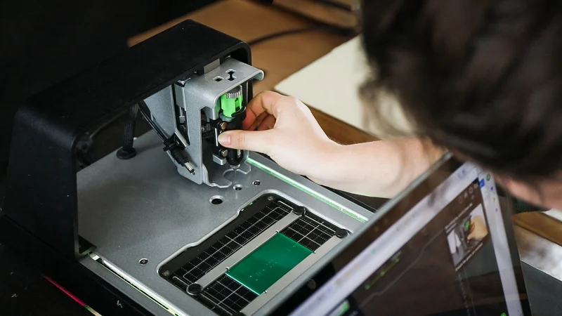
The V-One is a sub-$10k system designed to accelerate the prototyping of PCBs. The desktop printer is based on an intuitive design and can be implemented in a range of environments, from classrooms, to electrical engineering labs, to R&D departments. The V-One integrates multiple different functions into a single system, including circuit printing (using a printhead and conductive inks), drilling, solder paste application, and reflow soldering directly on the print bed.[8] The V-One enables users to print PCB prototypes in as little as an hour, which can then be tested, tweaked, and validated for production. In short, it offers greater flexibility and efficiency for the design and development of electronic circuit boards. Today, the V-One is used by product developers and educators in over 80 countries around the globe.
NOVA
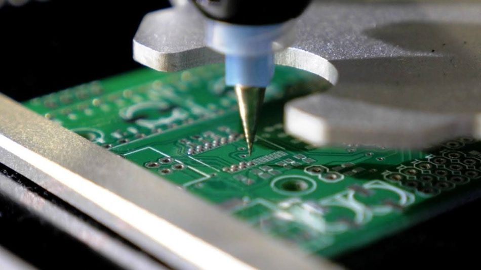
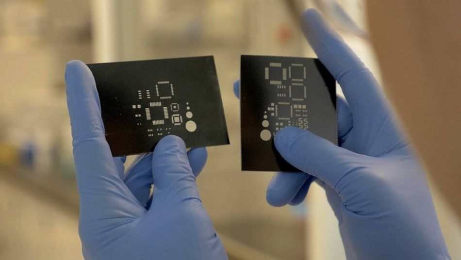
NOVA is Voltera’s solution for printing electronic circuits. Based on a modular direct-ink-write dispensing system, NOVA can print a wide variety of conductive and dielectric inks onto substrates to create both rigid and flexible printed electronics. With a configurable print area of up to 220 x 300 mm and the ability to print traces down to 100 microns in width, NOVA accommodates a range of printed electronics, from small sensors with fine details to those with large surface areas. The machine is also equipped with a vacuum table and customizable fixturing, which facilitates the use of flexible or irregular substrates.[9] Overall, Voltera’s NOVA allows users to rapidly iterate and produce highly complex electronic circuits and experiment in the development of new printed electronic capabilities.
Conclusion
Even as a relatively young technology, printed electronics are having a big impact, and there is no question that the low-cost production method for electronic circuits and sensors will continue to grow and evolve. Electronic printing technologies, such as Voltera’s V-One and NOVA systems, are vital to this growth. By making printed electronics more accessible and putting the technology into more people’s hands, Voltera is empowering researchers and innovators to explore and develop new applications for printed electronics.
Learn more about Voltera.Get in touch with Voltera to learn more about their electronic printing technologies. |
References
[1] TWI. “What is Physical Vapour Deposition?” 2023. Available from: https://www.twi-global.com/technical-knowledge/faqs/faq-what-is-physical-vapour-deposition-pvd
[2] PCB Directory. “What is PCB Etching?” April 24, 2020. Available from: https://www.pcbdirectory.com/community/what-is-pcb-etching
[3] Goosey M. Water use in the printed circuit board manufacturing process and approaches for reducing consumption. Circuit world. 2005 Jun 1;31(2):22-5. https://doi.org/10.1108/03056120510571815
[4] Sanchez-Duenas L, Gomez E, Larrañaga M, Blanco M, Goitandia AM, Aranzabe E, Vilas-Vilela JL. A Review on Sustainable Inks for Printed Electronics: Materials for Conductive, Dielectric and Piezoelectric Sustainable Inks. Materials. 2023 May 24;16(11):3940. https://www.ncbi.nlm.nih.gov/pmc/articles/PMC10253832/
[5] Lemarchand J, Bridonneau N, Battaglini N, Carn F, Mattana G, Piro B, Zrig S, Noël V. Challenges, Prospects, and Emerging Applications of Inkjet‐Printed Electronics: A Chemist's Point of View. Angewandte Chemie International Edition. 2022 May 9;61(20):e202200166. https://doi.org/10.1002/anie.202200166
[6] Chandrasekaran S, Jayakumar A, Velu R. A Comprehensive Review on Printed Electronics: A Technology Drift towards a Sustainable Future. Nanomaterials. 2022 Nov 29;12(23):4251. https://doi.org/10.3390/nano12234251
[7] Fu Z, Tanninen P, Keskinen J, Lev R, Leminen V, Mäntysalo M. Wear reliability and failure mechanism of inkjet-printed conductors on paperboard substrate. Flexible and Printed Electronics. 2023 Apr 24;8(2):025004. https://iopscience.iop.org/article/10.1088/2058-8585/accc9b/meta
[8] Voltera. “V-One” 2023. Available from: https://www.voltera.io/v-one
[9] Voltera. “NOVA” 2023. Available from: https://www.voltera.io/nova